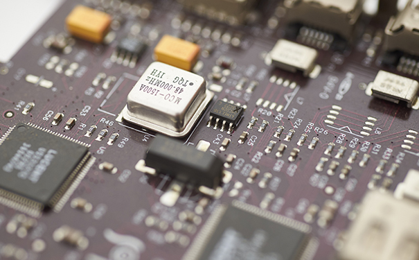
Chip resistor is one of the metallic glass uranium resistors. It is a resistor made of metal powder and glass uranium powder mixed and printed on the substrate by screen printing. Resistance to humidity and high temperature, low temperature coefficient. To help you understand in depth, this paper will summarize the relevant knowledge of chip resistors. If you are interested in the content to be covered in this article, please read on.

Basic parameters of chip resistor
There are five parameters of SMD resistance, namely size, resistance, tolerance, temperature coefficient and packaging.
1. The size series chip resistor series generally has seven sizes, which are represented by two size codes. One dimension code is the EIA (American Electronic Industry Association) code represented by four digits. The first two digits and the last two digits respectively represent the length and width of the resistance, in inches. The other is the metric code, which is also represented by 4 digits, and its unit is millimeter. The power rating varies with different sizes of resistors.
2. The nominal resistance of resistance series is determined by series. Each series is divided by the tolerance of resistance (the smaller the tolerance, the more the resistance value is divided), and the most commonly used one is E-24 (the tolerance of resistance value is ± 5%).
The resistance value is represented by three digits on the surface of the chip resistor, of which the first and second digits are the effective numbers, and the third digit represents the number of zeros. If there is a decimal point, it is represented by "R" and occupies one significant digit. Nominal resistance code representation method.
3. The tolerance of patch resistance (carbon film resistance) has 4 levels, namely F level, ± 1%; Grade G, ± 2%; Grade J, ± 5%; Class K, ± 10%.
4. Temperature coefficient The temperature coefficient of patch resistance has two levels, that is, w level, ± 200 ppm/℃; Grade X, ± lOOppm/℃. Only the resistance with tolerance of Class F can be Class x, and the resistance with tolerance of other classes is generally Class W.
5. There are two main types of packaging: bulk packaging and ribbon packaging.
The working temperature range of the chip resistor is - 55 -+125 ℃, and the maximum working voltage is related to the size: 0201 minimum, 0402 and 0603 is 50V, 0805 is 150V, and other sizes are 200V.
Precautions for using patch resistors
Before using the patch resistor, first check the appearance for obvious damage, such as lead breakage, cracking, burning, etc., and then use a multimeter to measure whether its resistance value is consistent with the nominal value. If the resistance value has changed, direct use will cause the circuit to work abnormally.
When using, pay attention to whether the rated power and working voltage of the resistor meet the design requirements. If the actual power exceeds the rated power of the resistor, the resistor will be heated and damaged.
If the actual working voltage is greater than the withstand voltage of the resistance, the resistance will break down and burn down. Resistors with rated power greater than 10W should be installed on a special bracket to make sure there is a certain heat dissipation space around them.
The surface treatment shall be carried out for the chip resistor before installation. The oxide layer on the surface of the pin shall be scraped off with a scraper blade or saw blade, and then tin plating shall be carried out to ensure the reliability of tin soldering and avoid false soldering (false soldering).
The pin of resistance in high-frequency circuit should not be too long, which can reduce the distribution parameters. The lead wire shall not be bent from the root during resistance welding of patch, otherwise it is easy to break.
During the storage and use of the patch resistor, the integrity of the paint film shall be maintained. After the film of the patch resistor falls off, the moisture-proof property becomes poor, and the normal operation cannot be guaranteed.
When welding the patch resistor, the action should be fast. Do not heat the resistor for a long time to avoid the change of resistance value.
When installing the patch resistor, the orientation of the color ring should be consistent, and the resistance mark should also be upward in case of the direct marking method, so as to facilitate inspection and maintenance. For resistors with larger power, screws and brackets shall be used to fix them to prevent the lead from breaking or causing short circuit.

