Integrated storage and computing or in memory computing is the complete integration of storage and computing, directly utilizing memory for data processing or computation. Under the traditional von Neumann architecture, data storage and computation are separated. Due to the increasing performance gap between storage and computation, the speed at which the processor accesses stored data is much lower than the processor's computation speed. The energy consumption of data transportation between memory and main memory is also much higher than the energy consumed by the processor's computation.
From the architecture design of NPU and TPU, it can be seen that their essence is to solve the problem of efficient data access, with only slight differences in implementation methods. In summary, it mainly includes:
By increasing communication bandwidth, high-speed data transmission and reducing power consumption can be achieved.
Store data as close as possible to the computing unit to reduce data handling latency and power consumption, such as multi-level caching and on-chip storage.
Improve the efficiency of data reuse in both time and space, and reduce the number of communication between data and main memory.
The integration of storage and computing enables the storage unit to have computing power by integrating the computing and storage units on the same chip, which greatly reduces the latency and power consumption caused by data handling. It is particularly suitable for deep learning scenarios that require large-scale data handling and large-scale parallel computing.
In store calculation
In memory computing generally includes two implementation methods: digital computing and analog computing. Analog computing has high energy efficiency but low computational accuracy, while digital computing has high computational accuracy but high power consumption. Currently, the mainstream in memory computing mainly relies on analog computing.
Analog in memory computing is mainly based on physical laws to implement multiplication and addition operations on memory arrays. Taking the matrix multiplication MxN on a memristor as an example, before the operation, the matrix M is stored in the memristor in row and column positions. The input matrix M is represented by different voltage values. According to Ohm's law and Kirchhoff's law, the corresponding multiplication and addition current vectors can be obtained at the output end. Multiple memory arrays can be paralleled to complete multiple matrix multiplication calculations.
Digital in memory computing is the process of adding logical computing circuits such as AND or gates, multipliers, and adders to a storage array, enabling it to not only have storage functions but also computational capabilities. Due to the need to add logic circuits to each storage unit, it does not have an advantage in chip area, which limits its expansion of computing power. Therefore, the current implementation of digital in memory computing relies more on advanced technology. Due to factors such as technology and cost, its application range is greatly limited.
Brain like computing
The pulse neural network (SNN) based on the human brain's pulse simulation computing framework is expected to achieve artificial intelligence while reducing the energy consumption of computing platforms.
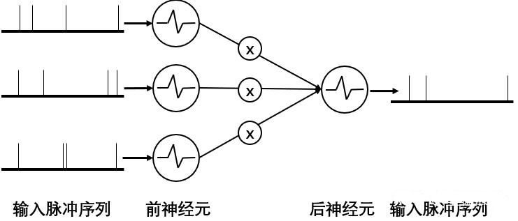
In the SNN model, the upstream neural pulse Vi is regulated by the synaptic weight Wi, and the synthesized current generated within a given time is equivalent to a dot product operation. From the legend, it can be seen that pulse computing simulates the neural computing process through the input and output of current. The entire system is event driven, and deep learning network computing is highly sparse. Therefore, through pulse communication and computing, large-scale parallel computing can be achieved at extremely low energy consumption.

Example diagram of pulse calculation
From the process of pulse computing, it can be seen that the hardware structure of pulse computing requires an integrated system design that tightly places neurons and synaptic arrays together. So currently, pulse neural network chips are mostly designed with an integrated architecture that simulates in memory computing.
Technical challenges
Although in memory computing has many advantages, it still faces many challenges in commercial applications. It still faces many problems and breakthroughs in device research and development, circuit design, chip architecture, generation manufacturing, EDA toolchain, and software algorithms, and the overall technical maturity is weak.
The integration of storage and computing needs to meet the design requirements of both storage and computing, such as the reliability of storage units, number of erasures, device consistency, and the response speed and power consumption of computing units. From the current semiconductor circuit design and manufacturing process, it is difficult to simultaneously consider the difficulties.
Due to limitations in process and chip area, the current commercial in memory computing chips have relatively low computational power and limited support for computing power and operators. Therefore, the neural network algorithms that can support them are also limited and have poor universality.
The current mainstream analog memory computing has poor computational accuracy, and inaccurate calculation results can lead to deviations between actual and ideal results. Although the calculation accuracy of digital memory is high, the computational cost is high.
The current implementation of logic unit circuits is mainly based on precise binary digit operations, while analog operations are relatively lacking in theory and circuit implementation, resulting in high difficulty in chip implementation of analog calculations.
The design of in memory computing chips differs significantly from conventional chips, and existing EDA tools cannot provide a standard unit library for chip designers to use. The lack of rapid development tools for large-scale memory arrays leads to low productization efficiency.
Solemnly declare that the article only represents the author's views and does not represent the views of our company. The copyright of this article belongs to the original author, and the reprint of the article is only for the purpose of disseminating more information. If the author's information is marked incorrectly, please contact us immediately to modify or delete it. Thank you for your attention!

