Since Google launched the first generation self-developed artificial intelligence chip Tensor Processing Unit (TPU) in 2016, it has been upgraded to the fourth generation TPU v4 after several years of development (as of the end of 2022). The TPU architecture design also achieves efficient computation of network layers such as deep learning convolutional layer and fully connected layer by efficiently parallelizing a large number of multiplication and accumulation operations.
Pulsating array
A systolic array is an array network composed of a large number of tightly coupled PEs, which is an architectural design for data flow. Each PE in a pulsating array communicates with one or more neighboring PEs for data communication. The functions of PEs are relatively simple, and the system achieves efficient computation through parallel computation of a large number of PEs. By maximizing the flow of data between different PEs, data reuse is achieved and the number of memory accesses during the computation process is reduced, which not only saves memory bandwidth but also reduces power loss caused by memory access.
In the operation process of traditional computing systems, the processing unit PE first reads data from the main memory, then performs the operation. After the operation is completed, the results are written back to the memory. Therefore, the speed of memory access is known as the bottleneck of the entire system's processing performance. Compared to the CPU using multi-level caching to solve the bottleneck problem of memory access speed, the pulsating architecture allows data to flow in different processing units to reduce the performance bottleneck caused by accessing main memory. As shown in the figure, in the operation process of a one-dimensional pulsating array, data first enters the first PE from main memory, is processed, and then passed to the next PE. At the same time, the next data enters the first PE, and so on. The data flows between different PEs until all calculations are completed before returning to main memory. So the pulsating array architecture achieves multiple reuse of input data, eliminating the process of data being written back to main memory before being read, and reducing the number of accesses to main memory. Therefore, the pulsating array can achieve high throughput with a small memory bandwidth.
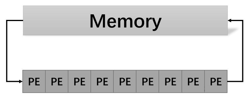
Systolic
The pulsating array architecture has the following characteristics:
1.PE has a simple functional structure, low implementation cost, and can integrate a large number of PEs to improve parallel computing capabilities.
2.A one-dimensional, two-dimensional, or tree array structure composed of a large number of isomorphic PEs, which can be flexibly expanded.
3.Pipelined data communication is used between different PEs to achieve efficient data reuse.
4.Data can only flow between adjacent PEs and is only suitable for specific algorithms, such as matrix operations, convolutions, etc.
TPU architecture design
TPU uses a pulsating array architecture design, where data is fed into the PE in the array at fixed time intervals in different directions for computation. After multiple steps of calculation, the results are finally summarized and output. Pulsatile arrays are only suitable for very simple and regular operations, while matrix multiplication and convolution precisely conform to the operational characteristics of pulsatile arrays.
The implementation of the pulsating array structure of the first generation TPU is shown in the figure. Similar to the GPU, the TPU is connected to the host CPU through the PCI-E bus, and the instructions of the TPU are encoded by the CPU to simplify hardware design and debugging. Matrix Multiply Unit (MXU) is the main computing unit, whose main function is to perform matrix multiplication operations. There are three data buffer areas with different functions around the matrix multiplication unit, as well as dedicated Activity, Normalize, and Pool units. The three data buffer areas are used for caching Weight FIFO, Unified Buffer (UB), and Accumulator (Acc), respectively.
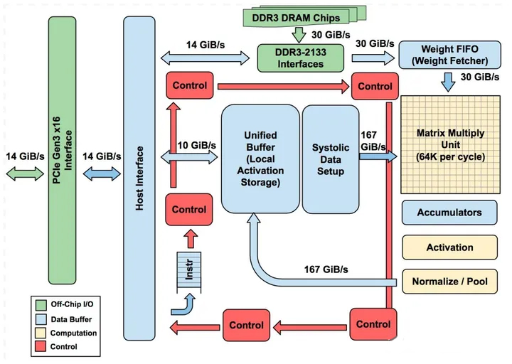
TPU architecture
During specific execution, instructions and data enter the TPU from the host interface. Weight parameters with higher reuse rates are preloaded into the Weight FIFO, and input data is loaded into the unified buffer UB. After completing the matrix multiplication operation in the matrix multiplication unit, the input data and weight parameters are sent to the accumulation unit Acc. After the Acc completes the part and accumulation, according to the model design needs, choose whether to send it to the Activity, Normalize, and Pool units for corresponding operations, and finally send the results back to the unified buffer UB.
In the layout of the first generation TPU hardware, the matrix multiplication unit and activation unit account for a total of 30% of the area. The matrix multiplication unit (MXU) has 256x256 MACs, and can complete 256x256 8-bit data multiplication and addition operations per clock cycle. Acc is a 32bit accumulator with a size of 4MiB. The size of UB is 24MiB, accounting for 29% of the area. It can directly interact with the Host CPU through DMA and be used to cache input data or save intermediate calculation results. The depth of the Weight FIFO is 4, and the weight parameters are read from off chip memory.
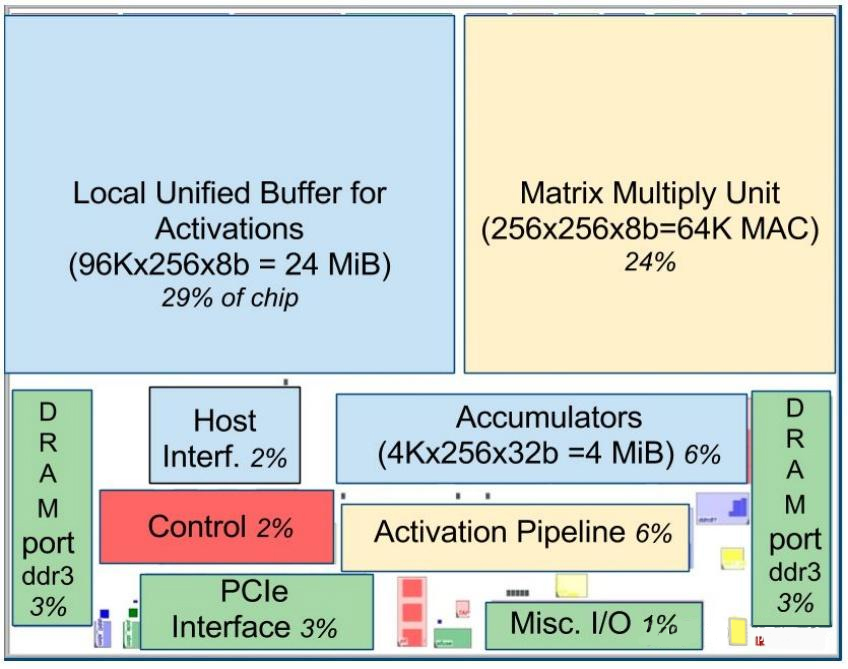
TPU layout
Matrix Multiply Unit (MXU) is a typical pulsating array, as shown in the figure, with weight flowing from top to bottom and data flowing from left to right. The input pixel data enters from the left side of the multiplication matrix and propagates from left to right to reuse the intermediate data. As the weights are preloaded, the product result can be quickly calculated as the input data advances, and the next step of accumulation calculation can be carried out through the control path.
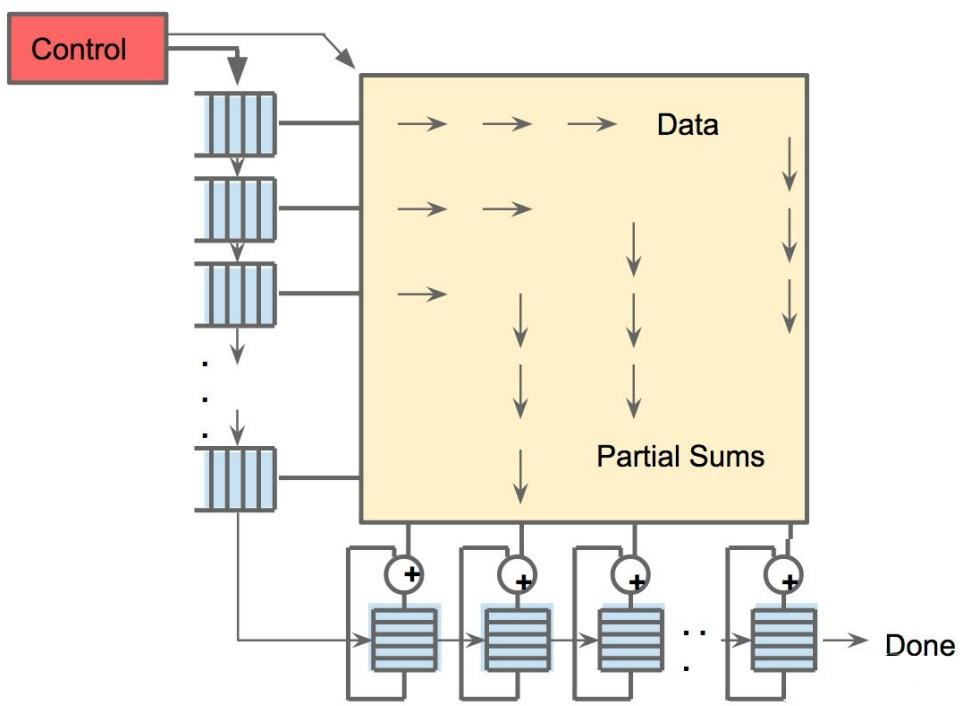
Matrix Multiplication Unit Data Flow
TPU architecture evolution
TPU v1 is Google's first generation AI dedicated chip, mainly focused on processing inference tasks. After launching TPU v1 for inference, Google began developing and designing a second generation TPU for training. Compared to TPU v1, TPU v2 has the following improvements:
1.TPU v2 has two Tensor Cores per chip.
2.Change the fixed activation pipeline to a vector unit with higher programmability.
3.Replace the cache in Accumulator and Activation Storage with a Vector Memory.
4.The matrix multiplication unit, as a coprocessor for vector units, is directly connected to the vector unit, increasing its programmability.
5.Replacing DDR3 with HBM and connecting it to vector storage can provide higher bandwidth and read/write speed.
6.Add an interconnect module between HBM and vector storage area to provide stronger scalability for connection between TPUs.
7.Added Scalar Unit, Transpose/Permute Unit, and other units to accelerate hardware for operations such as Transpose.
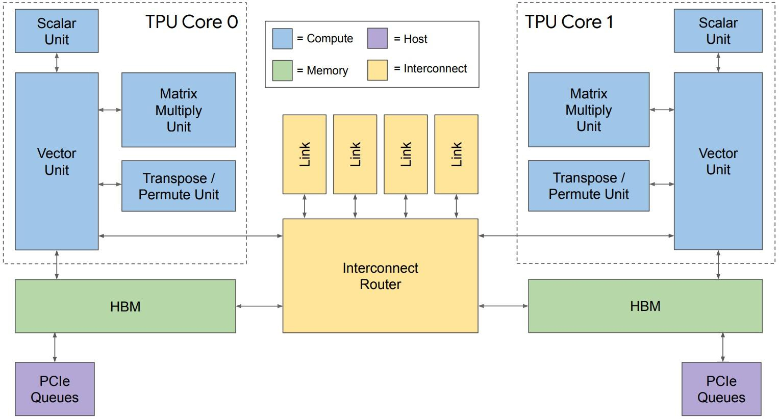
TPU v2 architecture
TPUv3 has further improved performance on the basis of TPUv2, with a 30% increase in clock frequency, memory bandwidth, and inter chip bandwidth. The number of matrix multiplication units MXU has doubled, the capacity of HBM has doubled, and the number of connectable nodes has increased fourfold.

TPU v1 v2 v3 architecture differences
Due to cost considerations, Google has designed TPU v4 separately for training and for driving TPU. TPU v4 for training has two Tensor Cores, while PU v4i for inference only has one Tensor Core, balancing universality, performance, and cost. In TPU v4i, a single Tensor Core contains four matrix multiplication units MXU, which is twice the size of TPU v3. Google has also added a performance counter in the design of TPU v4i to assist the compiler in better understanding the operation of the chip.
Solemnly declare that the article only represents the author's views and does not represent the views of our company. The copyright of this article belongs to the original author, and the reprint of the article is only for the purpose of disseminating more information. If the author's information is marked incorrectly, please contact us immediately to modify or delete it. Thank you for your attention!

