The Cambrian period was one of the earliest AI chip companies in China to study. The design of their AI chip NPU (Neural Network Processing Unit) originated from a series of early AI chip architecture studies, mainly including DianNao, DaDianNao, PuDianNao, ShiDianNao, Cambricon-X, and other research achievements.
DianNao
DianNao is a pioneering research in AI chip design, designed specifically for processing large-scale deep learning network operations. As shown in the figure, the chip adopts a modular design that is separated from each other, mainly consisting of three parts: Control Processor (CP), Neural Functional Unit (NFU), and on-chip storage module. Among them, the on chip storage module is further divided into NBin for storing input data, NBout for storing output data, and SB for storing neural network model weight parameters. These three storage blocks are all on chip storage to achieve low latency and low power consumption.
At present, the number of parameters in deep learning networks is very large, and the size of the on-chip cache area is generally much smaller than the number of parameters, making it impossible to store all the parameters of the entire network on the chip. So the DianNao architecture design adopts a time-sharing reuse method, where only a portion of the network is loaded and executed each time. The model parameters are loaded into SB in batches, and the input data of each network layer is also loaded into NBin batches. The calculation results of each layer are written into NBout. NFU (Neural Functional Unit) is a computing unit composed of a three-level pipeline, mainly responsible for completing the core computing logic of neural networks, such as multiplication, addition, and nonlinear function transformation.
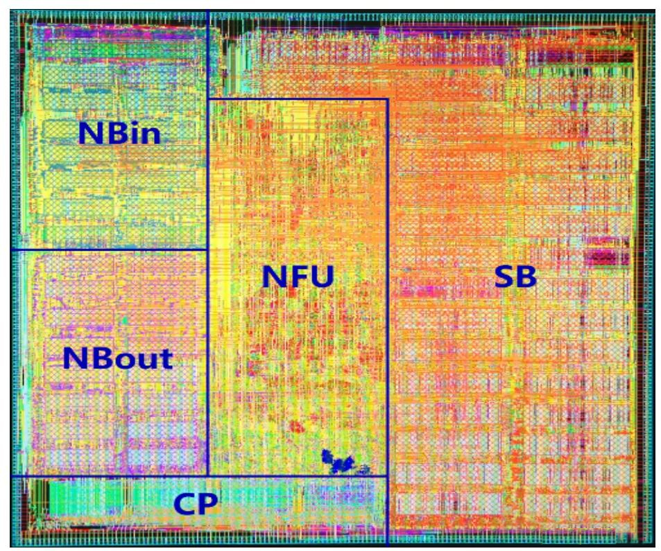
Diannao layout(65nm)
The design divided into different modules can find a better design balance point in terms of power consumption and performance. The input storage (NBin), weight storage (SB), and output storage (NBout) are implemented separately. On the one hand, different transmission bandwidth can be set according to different data access characteristics, and on the other hand, cache like functions can be realized, that is, the processor can calculate the current set of data at the same time, The loading of the next set of data or parameters can be initiated through DMA. As shown in the figure, each storage unit is equipped with a DMA and an instruction cache FIFO, which decouples the calculation process and data transmission process to achieve efficient data prefetching. As long as the previous instruction finishes using the data, the next instruction can start data transmission without waiting for the calculation of the previous instruction to be completed.
The computing unit NFU consists of three stages and is executed in a pipeline form, which is the core computing module of the neural network. NFU-1 is a 16x16 parallel multiplication unit, which can perform 256 multiplication operations simultaneously in one cycle. NFU-2 contains 16 addition trees, each adder containing 15 adders, arranged in a structure of 8-4-2-1, and NFU-3 contains 16 activation function units. Overall, all resources of NFU are divided into 16 parts. Each part of NFU-1 contains 16 multipliers, which are executed simultaneously to obtain 16 multiplication results. Then, they are fed into the addition tree of NFU-2. In each addition tree, 8 adders perform addition operations on 16 numbers to obtain 8 results. Based on this, 4-2-1 adders perform addition operations on the previous results, and finally, a cumulative result is obtained, which is then fed into the activation unit of NFU-3 for calculation.
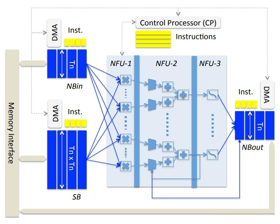
Diannao Architecture
DaDianNao
DaDianNao has proposed a chip architecture for mainstream neural network models that can accommodate larger models, mainly targeting high-performance AI training and inference computing tasks on the server side. Although the DianNao architecture has achieved significant improvements in performance and power consumption compared to CPUs, it also has some issues and limitations. DianNao mainly uses three on-chip buffers (NBin, SB, NBout) for data partitioning processing, storing different types of data blocks in different on-chip storage. It can be targeted and optimized based on the characteristics and reuse of different types of data, achieving optimal data transfer times and efficiency between the chip and main memory, thereby improving the overall performance of the chip and reducing power consumption. DaDianNao is an AI chip architecture designed to handle large-scale neural network models. It adopts a multi chipset design based on tiles and nodes to solve the bandwidth and power consumption problems caused by the communication of parameters of large models between chips and memory.
As shown in the figure, each tile contains one NFU, four eDRAM Banks, and an I/O interface connected to the central eDRAM. The model parameters are stored in the eDRAM storage area closer to the NFU, and the input and output data need to be loaded through memory access operations. Tile uses eDRAM instead of SRAM to store model parameters, achieving a better balance between storage density, access latency, and power consumption for the resource requirements of large
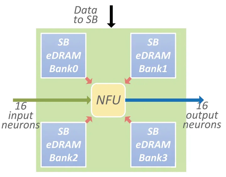
tile architecture
When the parameters of the model are much larger than the input/output data, the large-sized model parameters are deployed in eDRAM closer to the computing component to reduce memory access latency during the calculation process. Loading smaller input/output through memory access operations can reduce effective memory access overhead, and splitting and placing SB to reduce data access conflicts and further reduce memory access latency.
Compared to DianNao, DaDianNao's NFU is more complex and has added functional modules designed for model training. The improved NFU calculation unit is shown in the figure. The intermediate values calculated in each tile will be placed in the local eDRAM of the tile, and will be output after the calculation is completed.
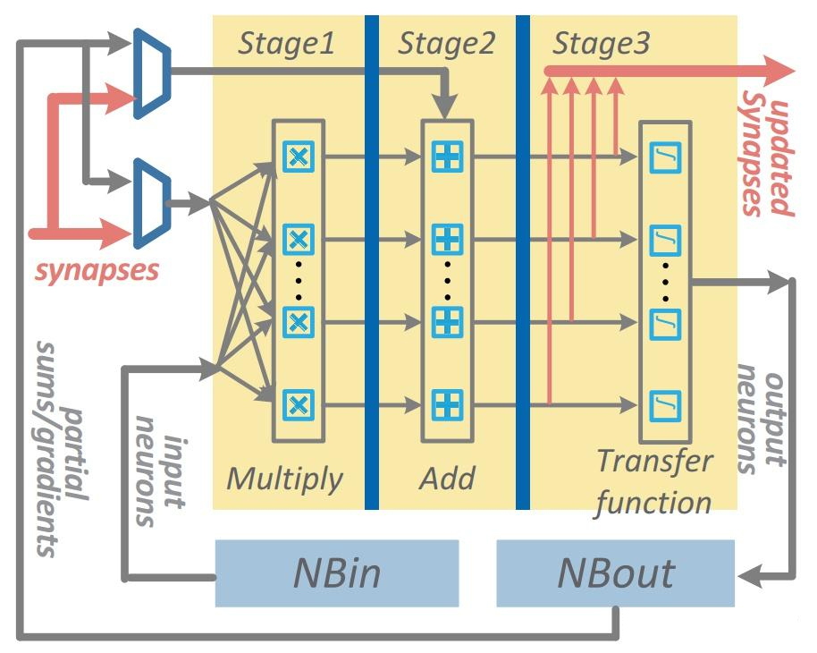
DaDianNao NFU architecture
In a multi chipset, a chip is a node, as shown in the figure. A node contains 16 tiles and two central eDRAM banks, which are connected to each other through Fat-trees. One of these two central eDRAM storage areas is used to broadcast input data to each tile, and the other is used to collect the output results of all tiles.
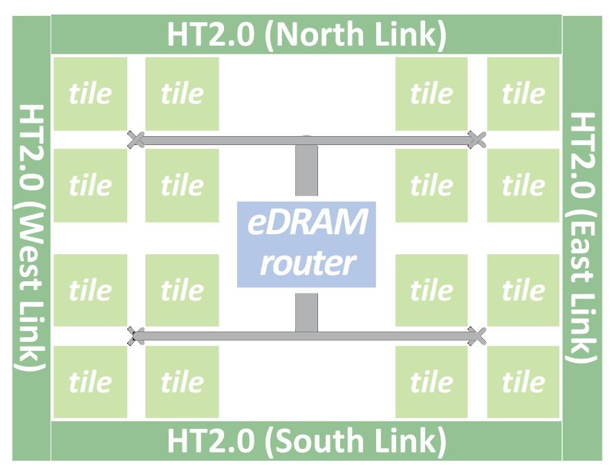
node structure
In a multi chip system, four sets of HyperTransport 2.0 communication channels are integrated around each chip, which are used to connect the chip with the surrounding chips to form a multi chip system. Compared to DianNao, under the same computing power, its chip area is reduced by 28.5%. Storing parameters in eDRAM on the chip reduces the bandwidth requirement for off chip memory access. The parameter storage unit is placed closer to the NFU and stored in blocks, which not only reduces data access conflicts but also improves data transmission speed.
ShiDianNao
ShiDianNao is a specialized AI processor based on CNN model for real-time image acquisition and processing. The chip is directly connected to the image sensor, and image data can be directly input to the processing unit of the chip for processing without going through DRAM memory. As shown in the figure, the storage components in ShiDianNano are similar to DianNano, divided into NBin, NBout, and SB, which are used to store input data, output data, and weight parameters of the neural network, respectively. The computing unit includes a neural network-specific computing unit NFU and a universal logic computing unit ALU. ShiDianNao has introduced a buffer controller between the storage unit and the computing unit, which is used to cache input data and aggregate NFU calculation results to improve processor parallelism.

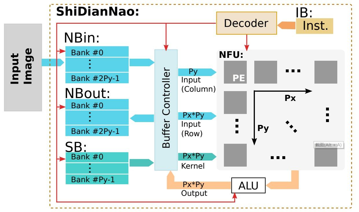
ShiDianNao architecture
The NFU in ShiDianNao is composed of a two-dimensional array of processing elements called Px * Py, which supports data flow between PEs. The NFU reads parameters and input data and distributes them to different PEs for processing. Afterwards, the NFU collects and summarizes the processed results, which are output to an ALU unit. The ALU contains hardware implementations of nonlinear activation functions, and the calculation results of the ALU are finally written to the NBout through the Buffer Controller.
Each PE unit also has an internal storage structure to support data transmission between PEs. As shown in the figure, each PE is composed of components such as a multiplier, an adder, several registers, and two sets of FIFO for data exchange. FIFO-H is used to store horizontal data, and FIFO-V is used to store vertical data. Each PE has three input interfaces, one for receiving control signal operand, one for receiving weight parameter Kernel, and one for receiving input data, which may come from the output of the right PE, the output of the lower PE, or NBin. Each PE has two outputs, one for writing the calculation results to NBout, and the other for transmitting to neighboring PEs to achieve data transmission between different PEs. Due to the large amount of duplicate data between adjacent sliding windows in convolutional operations, data transmission and multiplexing between PEs can be achieved by receiving data from adjacent PEs through two modules, FIFO-H and FIFO-V, which can greatly reduce the storage bandwidth requirement. Kernel data is sent to each PE in the form of broadcast for calculation.

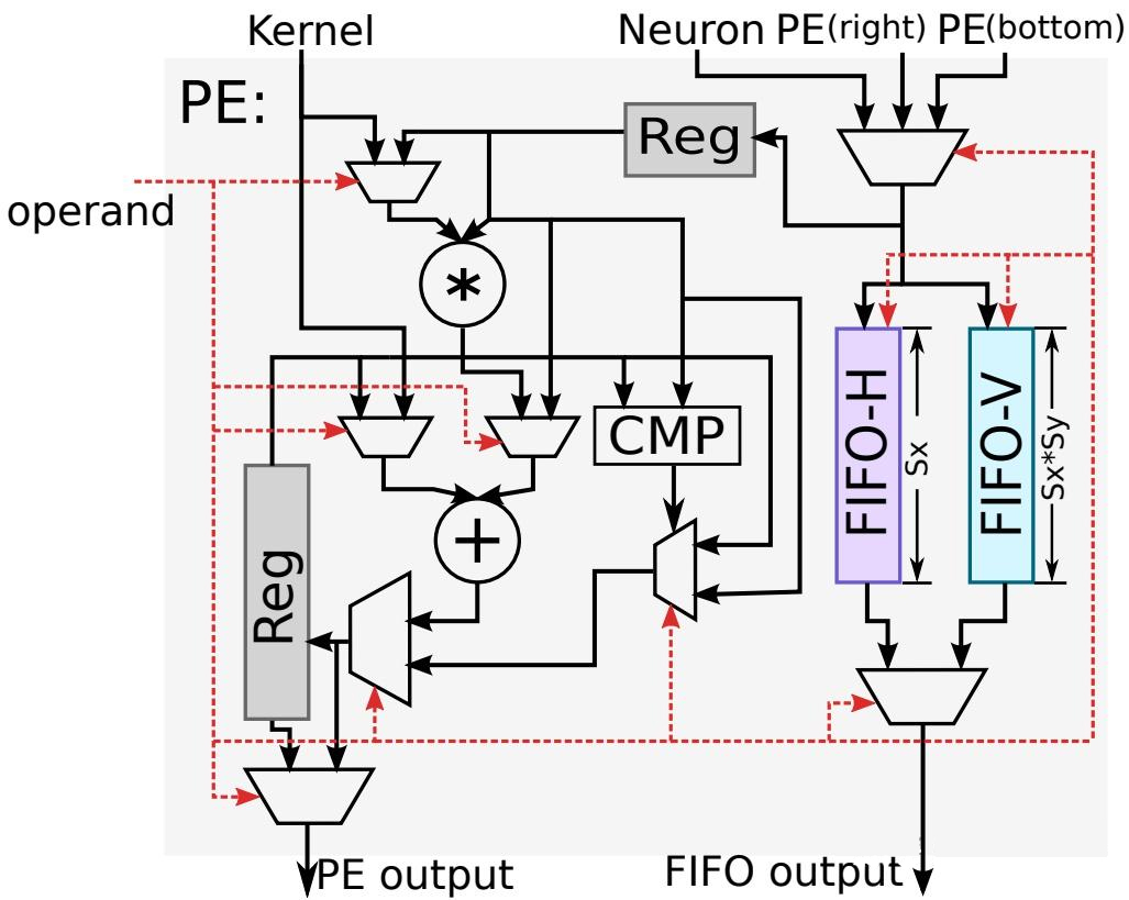
ShiDianNao PE architecture
PuDianNao
After analyzing the differences in memory access behavior and computing modes among various machine learning algorithms, PuDianNao redesigned it for finer grained data reuse and computing operations, enabling it to support AI processors that include seven classic machine learning algorithms, including KNN, DNN, SVM, and Classification Tree.
The architecture of PuDianNao consists of several FUS (Function Unit) units, three different purpose data cache modules (Hot Buffer, Cold Buffer, Output Buffer), one instruction cache module (Inst Buffer), and one control module (Control Module). Overall, based on the analysis and summary of different machine learning characteristics, PuDianNao improves overall computing performance by defining dedicated hardware, and improves memory access performance by designing specific cache modules.
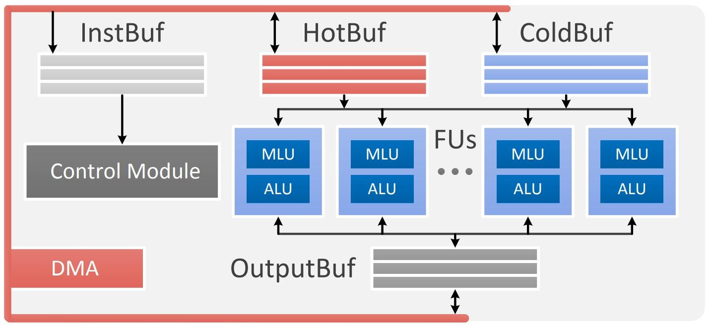
PuDianNao architecture
Cambricon-X
Cambricon-X is a chip architecture designed primarily for the sparsity characteristics of neural networks. There are two main types of sparsity in neural networks, one is the sparsity of weight parameters, and the other is the sparsity of feature vectors. Cambricon-X implements hardware support for weight sparsity, while feature vector sparsity dynamically changes with input data, making its management and control logic more complex. Therefore, Cambricon-X does not have hardware support for this aspect.
On the one hand, sparsity in neural networks can be improved through sparse training (such as adding regularization and gating functions during the training process) to increase the sparsity of model parameters, and on the other hand, pruning algorithms can further enhance the sparsity of the model. Han Song et al.'s research has shown that pruning techniques can remove more than 90% of the weight coefficients of deep learning network models without affecting the accuracy of model calculations. Although high sparsity of the model can be achieved algorithmically, this sparsity is often irregular. Currently, mainstream hardware platforms such as CPUs and GPUs are unable to effectively accelerate irregular sparsity, so performance is still greatly limited.
Cambricon-X proposes a hardware implementation scheme for efficient computation of sparse neural networks. As shown in the figure, the architecture design of Cambricon-X shares many similarities with the design of the DianNao series, mainly including the control processor CP, buffer controller, two data buffers NBin and NBout, memory access module DMA, and computing unit Computing Unit, where the computing unit is composed of multiple processing elements (PE). The main difference lies in the intermediate Buffer Controller module, which is specifically introduced for sparse accelerators and also implements the core of sparse memory access and computation.
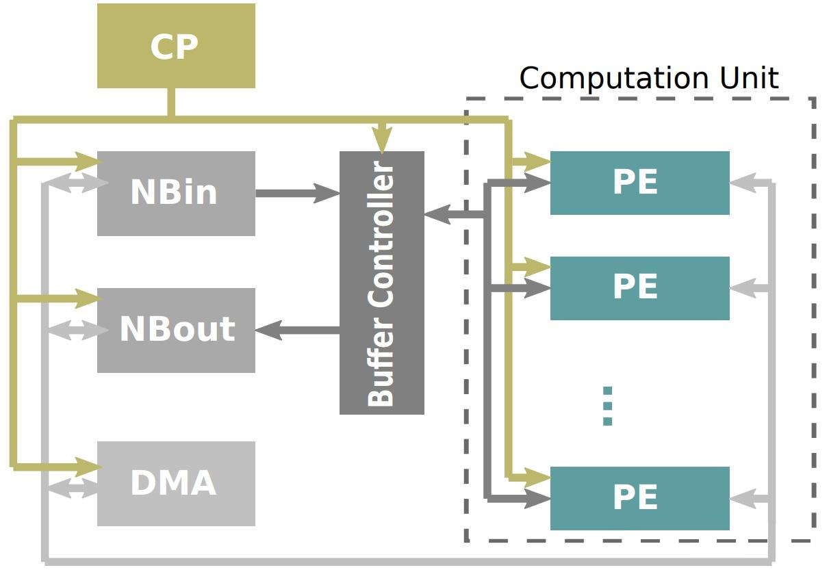

Cambricon-X architecture
Cambricon-X proposes a hardware implementation scheme for efficient computation of sparse neural networks. As shown in the figure, the architecture design of Cambricon-X shares many similarities with the design of the DianNao series, mainly including the control processor CP, buffer controller, two data buffers NBin and NBout, memory access module DMA, and computing unit Computing Unit, where the computing unit is composed of multiple processing elements (PE). The main difference lies in the intermediate Buffer Controller module, which is specifically introduced for sparse accelerators and also implements the core of sparse memory access and computation.
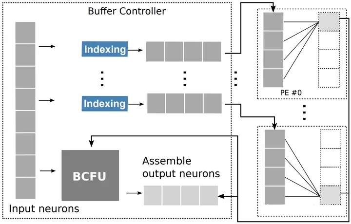
Buffer Controller architecture
The introduction of the IM module enables only the indexed data to be passed to the PE for subsequent calculation operations. On the one hand, the amount of indexed data accounts for a small proportion in the sparse network, which can greatly reduce the bandwidth requirement between the BC region and the PE. On the other hand, the indexed data completes data rearrangement in the BC region, requiring only a few parallel calculation operations on the PE.
PE is a neural network computing unit, as shown in the figure. SB is a parameter buffer used to cache the weight parameters of the network. Although on-chip storage space is limited and cannot load all weight parameters, weights have stronger repeated access characteristics. Therefore, SB design can still greatly reduce the cost of data access. PEFU is a hardware implementation of computational logic, essentially a combination of multipliers and adders required for neural network calculations.

Cambricon-X PE architecture
Summary
In summary, from the Diannao series and Cambricon X, NPU mainly achieves more efficient computing by adding more parallel computing units to AI computing, which has both data-intensive and computationally intensive characteristics. At the same time, it solves the problem of efficient data access by bringing computing closer to storage. Design AI chips for specific fields through software and hardware collaborative design based on different application scenarios and algorithm characteristics, and find the best balance between performance, power consumption, area, and other indicators.
Solemnly declare that the article only represents the author's views and does not represent the views of our company. The copyright of this article belongs to the original author, and the reprint of the article is only for the purpose of disseminating more information. If the author's information is marked incorrectly, please contact us immediately to modify or delete it. Thank you for your attention!

