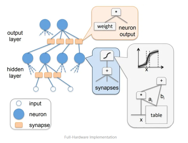
The simplest and most direct design approach for AI chips is to directly map neurons to hardware chips, as shown in the figure. The Full Hardware Implementation scheme maps each neuron to a logical computing unit and each synapse to a data storage unit. This architecture design can achieve a high-performance and low-power AI chip, such as an Intel ETANN chip. In the full hardware implementation scheme, the output data of the previous layer is multiplied by the weight, and the results of the multiplication are then added up, and then output to the next layer for calculation through an activation function. This architecture design tightly couples computing and storage, allowing the chip to avoid large-scale data access while performing high-speed computing, improving overall computing performance while also reducing power consumption.

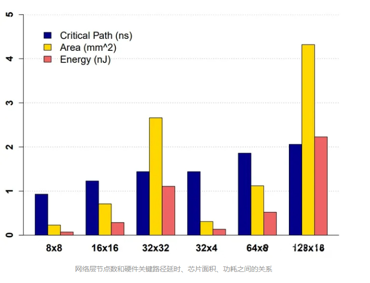
The full hardware implementation scheme has specific features such as simple design, high computational performance, and low power consumption, but it is only suitable for small-scale neural network calculations, and there are obvious hardware limitations for large-scale neural network calculations. As shown in the figure, when the nodes in the network layer are 16 x 16, the chip area only needs 0.71. However, when the nodes in the network layer are 32 x 32, the chip area needs 2.66. As the number of nodes in the network layer further increases, the required chip area and energy consumption will significantly increase. Therefore, the direct mapping scheme can no longer meet the growing scale of deep learning algorithm development.

The design of ASIC chips is basically focused on domain computing characteristics, optimized and designed around indicators such as memory access, energy consumption, throughput, cost, and flexibility. With the development of deep learning algorithms, the depth and scale of neural networks are becoming larger and larger. The network structure has gradually evolved from CNN based network architecture design to Transformer based network architecture design. The algorithm's demand for chips has also transitioned from computationally intensive to memory intensive, and the design of AI chips has also shifted from biased computing to a hybrid computing mode that integrates memory and computing. Specifically reflected in:
Underlying architecture: From separation of storage and computing to integrated design of storage and computing.
Data communication: From high-speed data communication to high-precision and sparse computing.
Model design: From model hardware independent design to model software hardware joint optimization design.
Time-domain computation
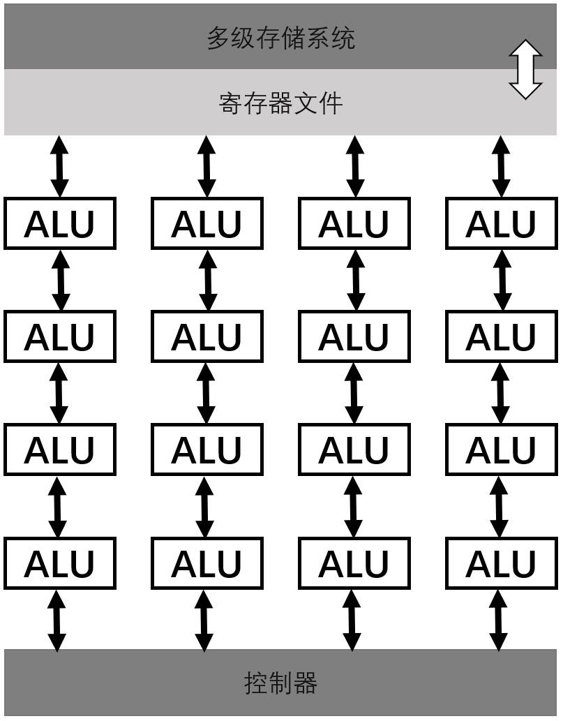
Time domain computing refers to a specialized processor that uses a customized instruction set, which manages and schedules the Arithmetic Logic Unit (ALU) and storage system through instruction pipelines. The ALU pipeline reads data from the storage system, undergoes multi-level pipeline processing, and writes the final calculation results back to the storage system. The deep learning neural network model mainly involves a large number of linear algebraic operations, while the control process is relatively simple. Therefore, AI chips usually adopt a highly parallel computing architecture design. In order to improve the parallel computing ability of the processor, it is necessary to have one instruction perform the same operation on multiple data elements simultaneously. Due to the relatively fixed computational process based on deep learning, the calculation of multiple fixed steps can be achieved efficiently through multiple ALU pipeline designs, such as the multiplication and accumulation of multiple data in matrix operations.

Time domain computing architecture
The DianNao series architecture design of the Institute of Computing Technology of the Chinese Academy of Sciences is a typical time-domain computing architecture design. The DianNao series of chips mainly consists of three parts: Neural Functional Unit (NFU), three different functional on-chip storage areas, and a controller. The NFU and storage are scheduled through the instructions of the controller, and the core NFU is divided into a three-level pipeline design of multiplication function segment NFU1, addition function segment NFU2, and nonlinear activation function segment NFU3 according to the convolutional operation process. DianNao has customized its design for the computational characteristics of deep learning, enabling it to achieve higher energy efficiency than general-purpose processors in AI computing.
Airspace computing
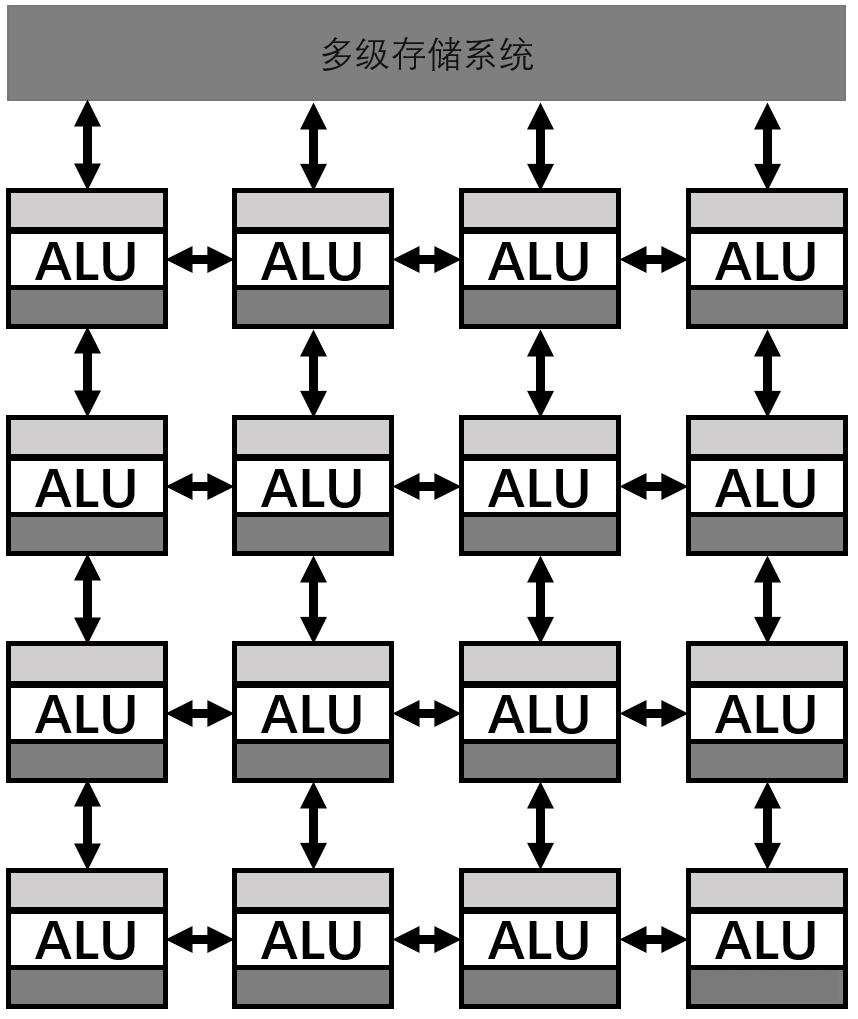
Unlike time-domain computing, each computing unit PE in spatial computing has independent control and storage units. The spatial computing architecture is usually composed of one-dimensional or two-dimensional PE arrays, each PE comes with its own controller and cache, and data can be directly transferred between PEs. In addition, there are multi-level storage systems composed of different levels of storage such as on chip global cache and off chip DRAM. The spatial computing architecture utilizes a large number of PE arrays to achieve efficient parallel computing, reducing the number of communications between processors and main memory through data flow between PEs.

Airspace computing architecture
Google TPU (Tensor Processing Unit) is one of the typical representatives of airspace computing architecture, which includes a two-dimensional matrix multiplication array consisting of 256x256 MACs. In addition, it also integrates normalization/pooling units and nonlinear activation units internally. The two-dimensional matrix multiplication array of TPU is interconnected in a systolic array manner. The data calculated by PE comes from the calculation results of adjacent PEs in the previous clock cycle, and the results calculated by PE in the current clock cycle flow into adjacent PEs in the same way to participate in the calculation in the next clock cycle, Due to the fact that the flow of data between different PEs in the array is transmitted and calculated according to a prescribed rhythm, just like blood pulsating through blood vessels, it is called a pulsating array architecture.
Data reuse
Data reuse refers to the repeated use of the same data during the calculation process to reduce the number of memory accesses. Data reuse in deep learning typically includes input data reuse, output data reuse, and weight data reuse. For example, in the DianNao architecture, SB and NBin are used to store weights and data neuron data, while NFU units are used for point multiplication and accumulation operations. The output data is stored in NBout, and during the calculation process, the output data is first output to the buffer until all partial sums are accumulated before being written back.
Storage optimization
The main ways to bridge the gap between computing units and memory include:
High bandwidth data communication technology, using more advanced communication technologies to improve the efficiency of data transmission.
By increasing on-chip storage capacity to bring data closer to the computing unit, the cost of data transportation between the computing unit and memory is reduced.
Using high-density on-chip storage technology, such as eDRAM storage cells composed of transistors and capacitors, has a higher storage density compared to SRAM.
Use 3D Integration memory technology to stack multiple blocks of memory vertically for greater storage capacity.
Directly implementing calculations within memory, that is, in memory calculations, is currently limited by manufacturing processes and calculation accuracy, and its application scope is still relatively limited.
Solemnly declare that the article only represents the author's views and does not represent the views of our company. The copyright of this article belongs to the original author, and the reprint of the article is only for the purpose of disseminating more information. If the author's information is marked incorrectly, please contact us immediately to modify or delete it. Thank you for your attention!

