Hi,welcome
86-755-88844016 6*12 hours online call
Analysis of Connector Manufacturing Process Flow
2023-05-22

Connector is one of the important components in electronic products, which is an important interface for connecting various electronic devices such as circuit boards, power supplies, and appliances to each other. The manufacturing process of connectors involves multiple links, including design, material selection, processing, assembly, and testing. This article will introduce the process flow and related manufacturing processes of connector manufacturing.


Connector manufacturing process flow


Stores reserve


The manufacturing of connectors requires a large amount of material support, including plastics, metals, electrode alloys, copper alloys, etc. At the beginning of the connector manufacturing process, these materials need to be prepared in advance.


Raw material processing


Next, the material needs to be processed, such as forming and welding metal materials, while plastic materials require injection molding, spraying, and other processes.


Part processing


Connectors are mainly composed of components such as connectors, sockets, shells, and shrapnel. These components require a series of processes such as drilling, milling, cutting, polishing, etc. during the processing process to assemble into the final connector product.


Assembling


After the parts of the connector are processed, they need to be assembled. This process requires assembling the parts one by one according to the instructions on the drawing. In addition, when connectors require waterproofing treatment, specialized waterproofing treatment processes are also required.


Testing


During the production process, connectors need to undergo multiple stages of testing, including material testing, processing testing, assembly testing, etc. These testing steps include multiple aspects such as electrical performance testing and mechanical performance testing.


Packing


Finally, the connector product after testing needs to be packaged and labeled, and then it will be sorted, stored, transported, and finally delivered to the customer's hands.
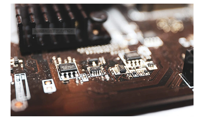
未标题-1

Manufacturing process


Injection molding


The plastic components in connectors are usually processed through injection molding technology, where the plastic is melted and injected into a steel mold for molding.


Metal stamping


Most metal parts in connectors need to be formed through metal stamping technology, using large punches and molds to punch the metal sheet into the shape of the required components.


Welding


Some electrode alloys in connectors require special welding processes due to their unique properties. Small components such as joints require manual electrode welding, while larger and thicker metal components typically require automation through equipment such as carbon arc welding or gas shielded welding.


Surface treatment


In order to enhance the corrosion resistance and aesthetics of connector products, surface treatment is usually required in the connector manufacturing process. For example, electrophoresis and anodizing not only enhance the corrosion resistance of metal surfaces, but also have good decorative effects.


The manufacturing process of connectors is very complex, including multiple links such as material preparation, raw material processing, part processing, assembly, testing, and packaging

Hot news
AUO
TFT-LCD modules, TFT-LCD panels, energy storage/management systems, touch solutions, etc.
The working principle and classification of electromagnetic voltage transformers
Electromagnetic voltage transformers are commonly used in power systems to measure voltage on high-voltage transmission lines. They can also be used to monitor the voltage waveform and amplitude in the power system, in order to timely detect faults and problems in the power system. In this article, we will provide a detailed introduction to the working principle and classification of electromagnetic voltage transformers.
Differences between thermal relays and thermal overload relays
Thermal relays and thermal overload relays are common electrical protection devices, but their working principles and protection objects are different. In this article, we will provide a detailed introduction to the differences between thermal relays and thermal overload relays.
Types and Packaging of Tantalum Capacitors
Tantalum capacitors are electronic components that use tantalum metal as the electrode material. They are usually divided into two types: polarized and unpolarized, and come in various packaging forms. In this article, we will discuss in detail the types and packaging of tantalum capacitors.
The difference between thermal relays and fuses
Thermal relays and fuses are common electrical components that play a protective role in circuits. Although they can both interrupt the circuit, there are some differences between them. In this article, we will provide a detailed introduction to the differences between thermal relays and fuses.
FT2232 Development Board
A development board designed with FT2232 chip, which fully leads out the IO port, can be used to design an interface expansion board based on this.
AI high-performance computing - integrated storage and computing
Integrated storage and computing or in memory computing is the complete integration of storage and computing, directly utilizing memory for data processing or computation. Under the traditional von Neumann architecture, data storage and computation are separated. Due to the increasing performance gap between storage and computation, the speed at which the processor accesses stored data is much lower than the processor's computation speed. The energy consumption of data transportation between memory and main memory is also much higher than the energy consumed by the processor's computation.
AI High Performance Computing - Google TPU
Since Google launched the first generation self-developed artificial intelligence chip Tensor Processing Unit (TPU) in 2016, it has been upgraded to the fourth generation TPU v4 after several years of development (as of the end of 2022). The TPU architecture design also achieves efficient computation of network layers such as deep learning convolutional layer and fully connected layer by efficiently parallelizing a large number of multiplication and accumulation operations.
AI High Performance Computing - Cambrian NPU
The Cambrian period was one of the earliest AI chip companies in China to study. The design of their AI chip NPU (Neural Network Processing Unit) originated from a series of early AI chip architecture studies, mainly including DianNao, DaDianNao, PuDianNao, ShiDianNao, Cambricon-X, and other research achievements.
AI High Performance Computing - AI Chip Design
The simplest and most direct design approach for AI chips is to directly map neurons to hardware chips, as shown in the figure. The Full Hardware Implementation scheme maps each neuron to a logical computing unit and each synapse to a data storage unit. This architecture design can achieve a high-performance and low-power AI chip, such as an Intel ETANN chip. In the full hardware implementation scheme, the output data of the previous layer is multiplied by the weight, and the results of the multiplication are then added up, and then output to the next layer for calculation through an activation function. This architecture design tightly couples computing and storage, allowing the chip to avoid large-scale data access while performing high-speed computing, improving overall computing performance while also reducing power consumption.
User Info:
Phone number
+86
  • +86
  • +886
  • +852
Company Name
Email
Product model
Quantity
Comment message