Hi,welcome
86-755-88844016 +852 2632 9637 6*12 hours online call
Isolation power supply uses a boost controller MAX668 to generate three isolation voltages for the slice power supply
2023-08-16

This application note shows a power supply that generates three isolation voltages for a slice. The isolation power supply uses a boost controller MAX668 with a flyback transformer for -24V and -72V outputs, and uses an optocoupler to isolate the feedback signal. The linear regulator MAX8867 provides a 3.3V output.


Some user line interface cards (SLICs) require power supply voltage to be isolated from local power sources. The circuit in Figure 1 generates three isolation voltages from a 5V input:+3.3V at 100mA, -24V at 100mA, and -72V at 25mA. It has a boost controller (U1) that operates in a transformer flyback topology and an optocoupler for isolating feedback signals. To provide this feedback (from -24V output to boost controller), the optocoupler (U4) is driven by a shunt regulator (U3) as an error amplifier.
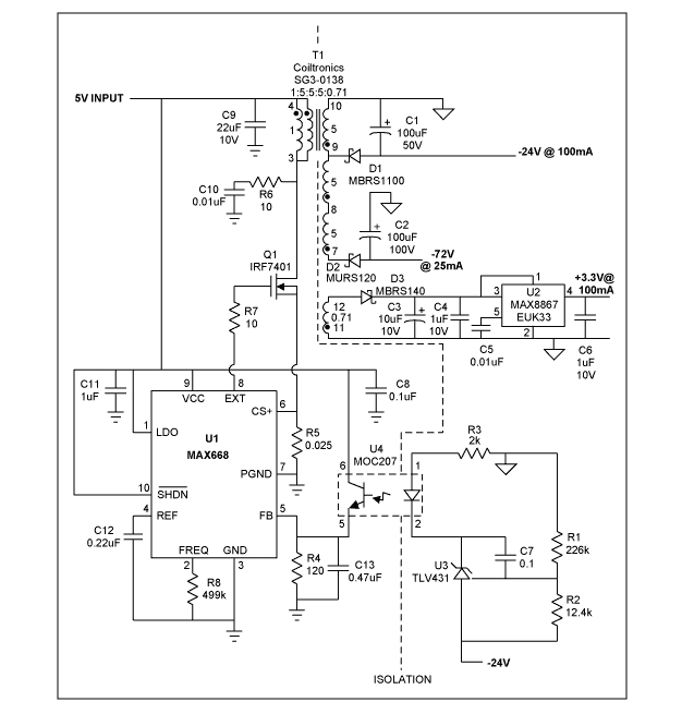
未标题-2

The SLIC power supply shown in Figure 1 uses a transformer to isolate three outputs (+3.3V, -24V, and -72V), and uses an optocoupler to isolate the feedback signal.


A custom transformer is required for a wide range of output voltage. Its core is a standard geometric coil SG3-0138 with a (L)=138nH/T ²。 The primary inductance is 6.8 µ H, and the peak current is 4A. The primary to secondary turn ratio is 1:5, so in order to achieve optimal efficiency, the duty cycle of the converter is close to 50%. The non regulated -72V output is derived from the regulated -24V output through three identical secondary windings connected in series. There is also a tap for -48V output, as well as a low-voltage winding that drives a linear regulator (U2) to provide+3.3V output. The winding specifications of the transformer are:


未标题-3


At the maximum specified load, the circuit outputs 5.0V at 1.138A,+3.28V at 103.9mA, -24.0V at 100mA, and -73.2V at 25.2mA, with an efficiency of 80%.


未标题-4


Note:


T1 wrapped around 138nH/T ² On the standard geometric core.


The primary inductance is 6.7 µ H.


Mainly on the 7th wheel and the 28th double track.


The secondary layer is three layers, with 35 times per layer and 32 times each time.


Low voltage secondary is 5 turns 32 #.


Declaration: The views expressed in this article only represent the author and do not represent the views and positions of ANSC. If there are any infringement or other issues, please contact our website for modification or deletion.

Hot news
AUO
TFT-LCD modules, TFT-LCD panels, energy storage/management systems, touch solutions, etc.
The working principle and classification of electromagnetic voltage transformers
Electromagnetic voltage transformers are commonly used in power systems to measure voltage on high-voltage transmission lines. They can also be used to monitor the voltage waveform and amplitude in the power system, in order to timely detect faults and problems in the power system. In this article, we will provide a detailed introduction to the working principle and classification of electromagnetic voltage transformers.
Differences between thermal relays and thermal overload relays
Thermal relays and thermal overload relays are common electrical protection devices, but their working principles and protection objects are different. In this article, we will provide a detailed introduction to the differences between thermal relays and thermal overload relays.
Types and Packaging of Tantalum Capacitors
Tantalum capacitors are electronic components that use tantalum metal as the electrode material. They are usually divided into two types: polarized and unpolarized, and come in various packaging forms. In this article, we will discuss in detail the types and packaging of tantalum capacitors.
The difference between thermal relays and fuses
Thermal relays and fuses are common electrical components that play a protective role in circuits. Although they can both interrupt the circuit, there are some differences between them. In this article, we will provide a detailed introduction to the differences between thermal relays and fuses.
FT2232 Development Board
A development board designed with FT2232 chip, which fully leads out the IO port, can be used to design an interface expansion board based on this.
AI high-performance computing - integrated storage and computing
Integrated storage and computing or in memory computing is the complete integration of storage and computing, directly utilizing memory for data processing or computation. Under the traditional von Neumann architecture, data storage and computation are separated. Due to the increasing performance gap between storage and computation, the speed at which the processor accesses stored data is much lower than the processor's computation speed. The energy consumption of data transportation between memory and main memory is also much higher than the energy consumed by the processor's computation.
AI High Performance Computing - Google TPU
Since Google launched the first generation self-developed artificial intelligence chip Tensor Processing Unit (TPU) in 2016, it has been upgraded to the fourth generation TPU v4 after several years of development (as of the end of 2022). The TPU architecture design also achieves efficient computation of network layers such as deep learning convolutional layer and fully connected layer by efficiently parallelizing a large number of multiplication and accumulation operations.
AI High Performance Computing - Cambrian NPU
The Cambrian period was one of the earliest AI chip companies in China to study. The design of their AI chip NPU (Neural Network Processing Unit) originated from a series of early AI chip architecture studies, mainly including DianNao, DaDianNao, PuDianNao, ShiDianNao, Cambricon-X, and other research achievements.
AI High Performance Computing - AI Chip Design
The simplest and most direct design approach for AI chips is to directly map neurons to hardware chips, as shown in the figure. The Full Hardware Implementation scheme maps each neuron to a logical computing unit and each synapse to a data storage unit. This architecture design can achieve a high-performance and low-power AI chip, such as an Intel ETANN chip. In the full hardware implementation scheme, the output data of the previous layer is multiplied by the weight, and the results of the multiplication are then added up, and then output to the next layer for calculation through an activation function. This architecture design tightly couples computing and storage, allowing the chip to avoid large-scale data access while performing high-speed computing, improving overall computing performance while also reducing power consumption.
User Info:
Phone number
+86
  • +86
  • +886
  • +852
Company Name
Email
Product model
Quantity
Comment message