Product Details
Overview
This chapter provides an overview of the microprocessor features, including the major functional components.
Key Features
A block diagram of the MCF528x and MCF521x is shown in Figure 1-1. The main features are as follows:
• Static Version 2 ColdFire variable-length RISC processor
— Static operation
— On-chip 32-bit address and data path
— Processor core and bus frequency up to 80 MHz
— Sixteen general-purpose 32-bit data and address registers
— ColdFire ISA_A with extensions to support the user stack pointer register, and four new instructions for improved bit processing
— Enhanced Multiply-Accumulate (EMAC) unit with four 48-bit accumulators to support 32-bit signal processing algorithms
— Illegal instruction decode that allows for 68K emulation support
• System debug support
— Real-time trace for determining dynamic execution path
— Background debug mode (BDM) for in-circuit debugging
— Real time debug support, with one user-visible hardware breakpoint register (PC and address with optional data) that can be configured into a 1- or 2-level trigger
• On-chip memories
— 2-Kbyte cache, configurable as instruction-only, data-only, or split I-/D-cache
— 64-Kbyte dual-ported SRAM on CPU internal bus, accessible by core and non-core bus masters
(e.g., DMA, FEC) with standby power supply support
— 512 Kbytes of interleaved Flash memory supporting 2-1-1-1 accesses
(256 Kbytes on the MCF5281 and MCF5214, no Flash on MCF5280)
– This product incorporates SuperFlash® technology licensed from SST.
• Power management
— Fully-static operation with processor sleep and whole chip stop modes
— Very rapid response to interrupts from the low-power sleep mode (wake-up feature)
— Clock enable/disable for each peripheral when not used
• Fast Ethernet Controller (FEC) (not available on the MCF5214 and MCF5216)
— 10BaseT capability, half- or full-duplex
— 100BaseT capability, half- or limited-throughput full-duplex
— On-chip transmit and receive FIFOs
— Built-in dedicated DMA controller
— Memory-based flexible descriptor rings
— Media-independent interface (MII) to transceiver (PHY)
• FlexCAN 2.0B Module
— Includes all existing features of the Freescale TouCAN module
— Full implementation of the CAN protocol specification version 2.0B
– Standard data and remote frames (up to 109 bits long)
– Extended data and remote frames (up to 127 bits long)
– 0–8 bytes data length
– Programmable bit rate up to 1 Mbit/sec
— Up to 16 message buffers (MBs)
– Configurable as receive (Rx) or transmit (Tx)
– Support standard and extended messages
— Unused message buffer (MB) space can be used as general-purpose RAM space
— Listen-only mode capability
— Content-related addressing
— No read/write semaphores
— Three programmable mask registers
– Global (for MBs 0-13)
– Special for MB14
– Special for MB15
— Programmable transmit-first scheme: lowest ID or lowest buffer number
— “Time stamp” based on 16-bit free-running timer
— Global network time, synchronized by a specific message
— Programmable I/O modes
— Maskable interrupts
• Three universal asynchronous/synchronous receiver transmitters (UARTs)
— 16-bit divider for clock generation
— Interrupt control logic
— Maskable interrupts
— DMA support
— Data formats can be 5, 6, 7, or 8 bits with even, odd, or no parity
— Up to 2 stop bits in 1/16 increments
— Error-detection capabilities
— Modem support includes request-to-send (URTS) and clear-to-send (UCTS) lines for two UARTs
— Transmit and receive FIFO buffers
• I2C module
— Interchip bus interface for EEPROMs, LCD controllers, A/D converters, and keypads
— Fully compatible with industry-standard I2C bus
— Master or slave modes support multiple masters
— Automatic interrupt generation with programmable level
• Queued serial peripheral interface (QSPI)
— Full-duplex, three-wire synchronous transfers
— Up to four chip selects available
— Master mode operation only
— Programmable master bit rates
— Up to 16 pre-programmed transfers
• Queued analog-to-digital converter (QADC)
— 8 direct, or up to 18 multiplexed, analog input channels
— 10-bit resolution +/- 2 counts accuracy
— Minimum 7 μS conversion time
— Internal sample and hold
— Programmable input sample time for various source impedances
— Two conversion command queues with a total of 64 entries
— Sub-queues possible using pause mechanism
— Queue complete and pause software interrupts available on both queues
— Queue pointers indicate current location for each queue
— Automated queue modes initiated by:
– External edge trigger and gated trigger
– Periodic/interval timer, within QADC module [Queue 1 and 2]
– Software command
— Single-scan or continuous-scan of queues
— Output data readable in three formats:
– Right-justified unsigned
– Left-justified signed
– Left-justified unsigned
— Unused analog channels can be used as digital I/O
— Low pin-count configuration implemented
• Four 32-bit DMA timers
— 15-ns resolution at 80 MHz (66 MHz for MCF5214 and MCF5216)
— Programmable sources for clock input, including an external clock option
— Programmable prescaler
— Input-capture capability with programmable trigger edge on input pin
— Output-compare with programmable mode for the output pin
— Free run and restart modes
— Maskable interrupts on input capture or reference-compare
— DMA trigger capability on input capture or reference-compare
• Two 4-channel general purpose timers
— Four 16-bit input capture/output compare channels per timer
— 16-bit architecture
— Programmable prescaler
— Pulse widths variable from microseconds to seconds
— Single 16-bit pulse accumulator
— Ability to boot from internal Flash memory or external memories that are 8, 16, or 32 bits wide (Continue..)
Product Description
| Type | Description |
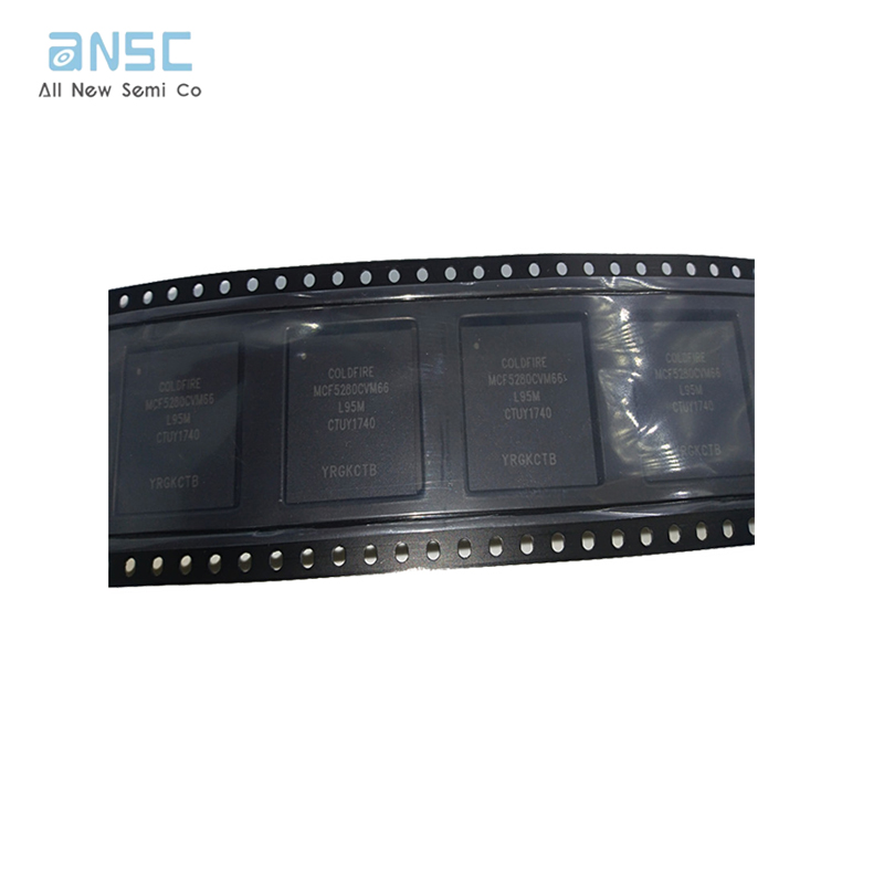
| ANSC PART# | ANSC - MCF5280CVM66 |
| Category | Integrated Circuits (ICs) |
| Embedded | |
| Microcontrollers | |
| Mfr | NXP USA Inc. |
| Series | MCF528x |
| Packaging | Tray |
| Part Status | Not For New Designs |
| DigiKey Programmable | Not Verified |
| Core Processor | Coldfire V2 |
| Core Size | 32-Bit |
| Speed | 66MHz |
| Connectivity | CANbus, EBI/EMI, Ethernet, I2C, SPI, UART/USART |
| Peripherals | DMA, LVD, POR, PWM, WDT |
| Number of I/O | 142 |
| Program Memory Size | - |
| Program Memory Type | ROMless |
| EEPROM Size | - |
| RAM Size | 64K x 8 |
| Voltage - Supply (Vcc/Vdd) | 2.7V ~ 3.6V |
| Data Converters | A/D 8x10b |
| Oscillator Type | External |
| Operating Temperature | -40°C ~ 85°C (TA) |
| Mounting Type | Surface Mount |
| Supplier Device Package | 256-MAPBGA (17x17) |
| Package / Case | 256-LBGA |
| Base Product Number | MCF5280 |
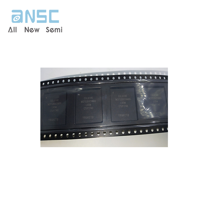
Product Photos
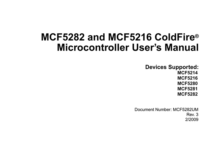
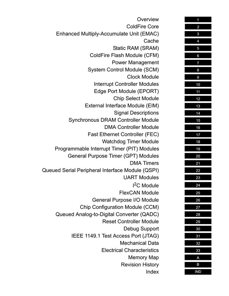
Product datasheet
For more information, please download
Payment&Transportation

Official Certificate&Certificate

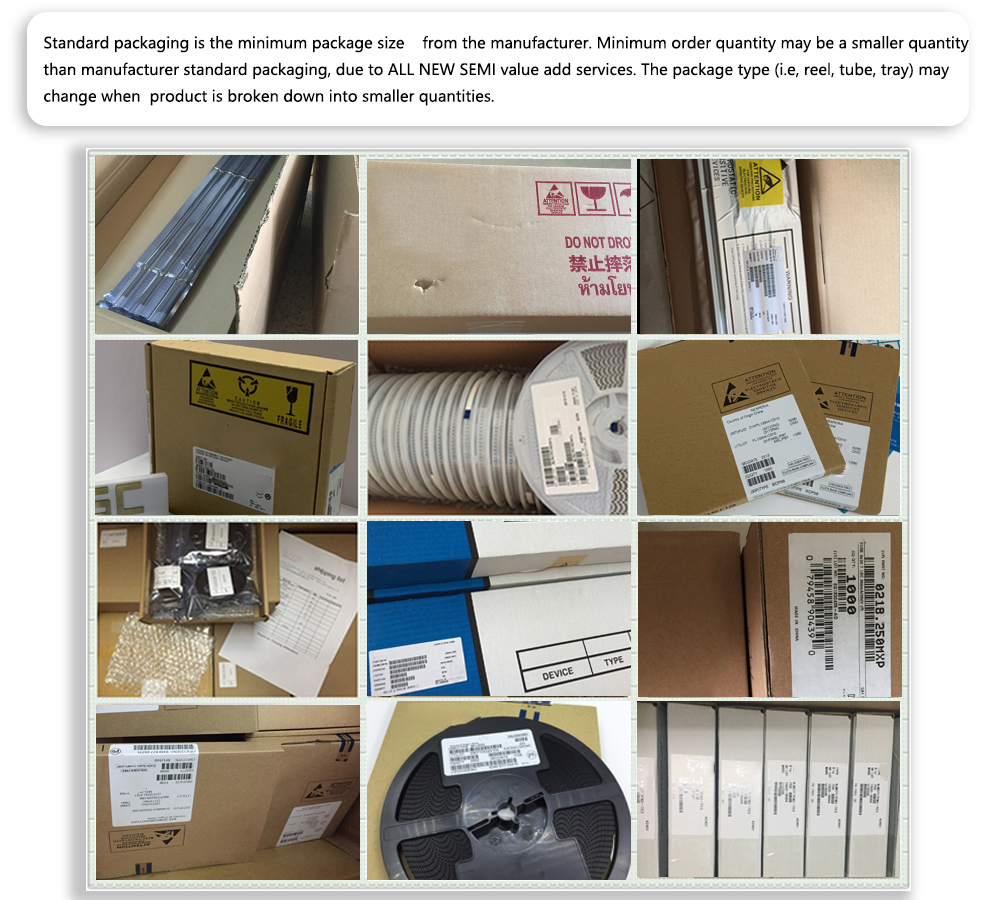
Standard packaging
Multiple product supply
Welcome to visit our company

Warehouse Real Shot

Hot Selling Product Recommendation
| Model | brand | quantity | package |
| BZX384-C5V1 | NXP | 6000 | SOD323 |
| SN74LVC1G123DCUR | TI | 2500 | VSSOP8 |
| V33MLA1206H | Littelfuse | 1000 | SMD1206 |
| FDS8958A | FAIRCHILD | 900 | SOP8 |
| MC2904DR2G | ON | 775 | SOP-8 |
| ICL3232IVZ | INTERSIL | 152 | TSSOP16 |
| IAM-82008-TR1 | AGILENT | 150 | SOP8 |
| NJM2882F03 | JRC | 100 | SOT23-5 |
| LP2988AIMX-3.0 | NSC | 22500 | SOP8 |
| TUSB522PRGER | TI | 52000 | QFN |
| NJM3717FM2 | JRC | 10500 | PLCC28 |
| OPA4322AIPWR | TI | 8500 | TSSOP14 |
| AT45DB321D-SU | ATMEL | 4900 | SOP8 |
| FDS8958A | FAIRCHILD | 3888 | SOP8 |
| DS2502P-500 | DALLAS | 3575 | SON-6 |
| PCA9500PW | NXP | 2500 | TSSOP16 |
| 20645-040T-01 | I-PEX | 1926 | CONN |
| SUD50P04-09L-E3 | VISHAY | 1670 | TO-252 |
| TL1431CPWR | TI | 1344 | TSSOP8 |
| PSMN3R0-30YLD | NXP | 980 | SOT669 |
| SG-615L14.7456MHZ | Epson | 945 | CRYSTAL OSCILLATOR |
| IRF7311TRPBF | IR | 942 | SOP-8 |
| MIC4827YMM | MICREL | 860 | MSOP-8 |
| S9S08RNA16M | FREESCALE | 759 | QFP32 |
| AD9884AKS-100 | ADI | 330 | QFP |
| ST4SI2M0020TPIFW | ST | 122 | DFN |
| MIC2505-2YM | MICROCHIP | 3525 | SOP8 |
| SSM3J351R,LXGF | TOSHIBA | 12000 | SOT23 |
| PBY160808T-601Y-N | CHILISIN | 8000 | SMD |
| R820T | RAFAEL | 200 | QFN-24 |
| SN74HCT573DWR | TI | 386 | SOP |
| NVTFS5116PLTAG | ON | 90 | WDFN-8 |
| ATXMEGA32A4U-ANR | MICROCHIP | 82000 | QFP44 |
| PIC16F18425-I/ST | MICROCHIP | 5260 | TSSOP14 |
| 80HCPS1848CRMI | IDT | 119 | BGA |
| BCM85110IFSBG | BROADCOM | 100 | BGA |
| WG82574IT S LBAC | INTEL | 78 | QFN64 |
| XC7VX1140T-1FLG1930I | XILINX | 60 | BGA |
| LMH0384SQE/NOPB | TI | 24 | WQFN-16 |
| XCVU19P-2FSVB3824E | XILINX | 10 | BGA |

