


Product Descriptions
The 1Gb DDR2 SDRAM is organized as a 32Mbit x 4 I/Os x 8banks, 16Mbit x 8 I/Os x 8banks or 8Mbit x 16 I/Os x 8 banks device. This synchronous device achieves high speed double-data-rate transfer rates of up to 800Mb/ sec/pin (DDR2-800) for general applications.
The chip is designed to comply with the following key DDR2 SDRAM features such as posted CAS with additive latency, write latency = read latency - 1, Off-Chip Driver(OCD) impedance adjustment and On Die Termination. All of the control and address inputs are synchronized with a pair of externally supplied differential clocks. Inputs are latched at the crosspoint of differential clocks (CK rising and CK falling). All I/Os are synchronized with a pair of bidirectional strobes (DQS and DQS) in a source synchronous fashion. The address bus is used to convey row, column, and bank address information in a RAS/CAS multiplexing style. For example, 1Gb(x8) device receive 14/10/3 addressing.
The 1Gb DDR2 device operates with a single 1.8V ± 0.1V power supply and 1.8V ± 0.1V VDDQ.
The 1Gb DDR2 device is available in 60ball FBGA(x4/x8) and in 84ball FBGA(x16).
Product Features
• JEDEC standard VDD = 1.8V ± 0.1V Power Supply
• VDDQ = 1.8V ± 0.1V
• 333MHz fCK for 667Mb/sec/pin, 400MHz fCK for 800Mb/sec/pin
• 8 Banks
• Posted CAS
• Programmable CAS Latency: 3, 4, 5, 6
• Programmable Additive Latenc y: 0, 1, 2, 3, 4, 5
• Write Latency(WL) = Read Latency(RL) -1
• Burst Length: 4 , 8(Interleave/nibble sequential)
• Programmable Sequential / Interleave Burst Mode
• Bi-directional Differential Data-Strobe (Single-ended data-strobe is an optional feature)
• Off-Chip Driver(OCD) Impedance Adjustment
• On Die Termination
• Special Function Support
- 50ohm ODT
- High Temperature Self-Refresh rate enable
• Average Refresh Period 7.8us at lower than TCASE 85°C, 3.9us at 85°C < TCASE < 95 °C
• All of products are Lead-Free, Halogen-Free, and RoHS compliant
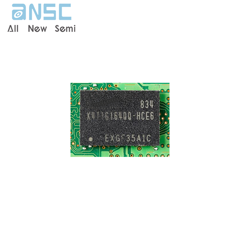
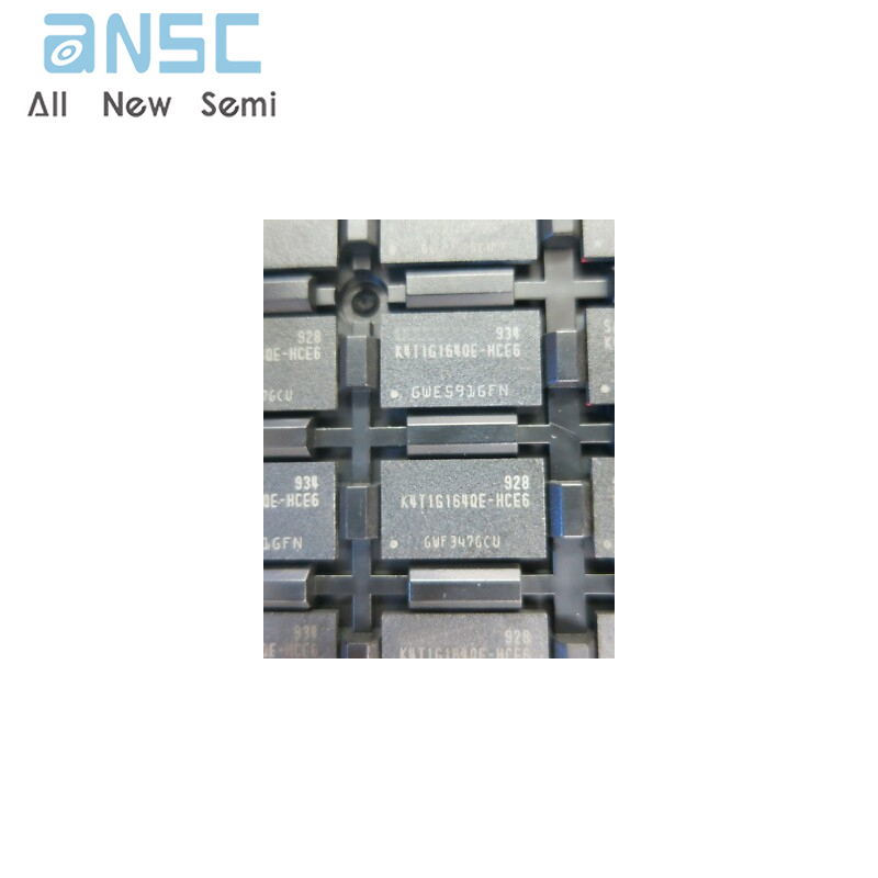
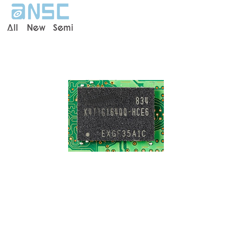
Product Photos
For more product information, please download the PDF