

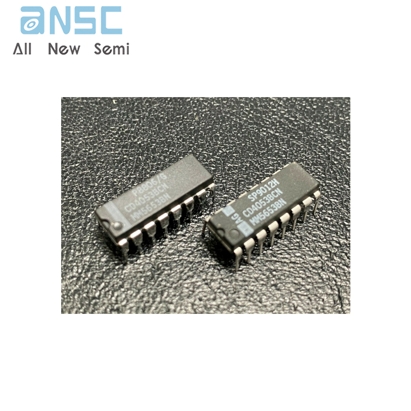

Product Descriptions
The CD4051BC, CD4052BC, and CD4053BC analog multiplexers/demultiplexers are digitally controlled analog switches having low “ON” impedance and very low “OFF” leakage currents. Control of analog signals up to 15Vp-p can be achieved by digital signal amplitudes of 3−15V. For example, if VDD = 5V, VSS = 0V and VEE = −5V, analog signals from −5V to +5V can be controlled by digital inputs of 0−5V. The multiplexer circuits dissipate extremely low quiescent power over the full VDD−VSS and VDD−VEE supply voltage ranges, independent of the logic state of the control signals. When a logical “1” is present at the inhibit input terminal all channels are “OFF”.
CD4051BC is a single 8-channel multiplexer having three binary control inputs. A, B, and C, and an inhibit input. The three binary signals select 1 of 8 channels to be turned “ON” and connect the input to the output.
CD4052BC is a differential 4-channel multiplexer having two binary control inputs, A and B, and an inhibit input. The two binary input signals select 1 or 4 pairs of channels to be turned on and connect the differential analog inputs to the differential outputs.
CD4053BC is a triple 2-channel multiplexer having three separate digital control inputs, A, B, and C, and an inhibit input. Each control input selects one of a pair of channels which are connected in a single-pole double-throw configuration.
Product Features
■ Wide range of digital and analog signal levels: digital 3 – 15V, analog to 15Vp-p
■ Low “ON” resistance: 80Ω (typ.) over entire 15Vp-p signal-input range for VDD − VEE = 15V
■ High “OFF” resistance:
channel leakage of ±10 pA (typ.) at VDD − VEE = 10V
■ Logic level conversion for digital addressing signals of 3 – 15V (VDD − VSS = 3 – 15V) to switch analog signals to 15 Vp-p (VDD − VEE = 15V)
■ Matched switch characteristics:
∆RON = 5Ω (typ.) for VDD − VEE = 15V
■ Very low quiescent power dissipation under all digital-control input and supply conditions: 1 µ W (typ.) at VDD − VSS = VDD − VEE = 10V
■ Binary address decoding on chip
Product Specification
| Attribute | Attribute value |
| ANSM-Part# | ANSM-CD4053BCN |
| Category | Integrated Circuits (ICs) |
| Interface | |
| Analog Switches, Multiplexers, Demultiplexers | |
| Manufacturer | - |
| Packaging | Tube |
| Part Status | Obsolete |
| Switch Circuit | SPDT |
| Multiplexer/Demultiplexer Circuit | 2:1 |
| Number of Circuits | 3 |
| On-State Resistance (Max) | 240Ohm |
| Channel-to-Channel Matching (Ron) | 5Ohm |
| Voltage - Supply, Single (V+) | 5V ~ 15V |
| Voltage - Supply, Dual (V±) | ±2.5V ~ 7.5V |
| Switch Time (Ton, Toff) (Max) | 320ns, 150ns |
| -3db Bandwidth | 40MHz |
| Current - Leakage (IS(off)) (Max) | 50nA |
| Crosstalk | -40dB @ 3MHz |
| Operating Temperature | -55°C ~ 125°C (TA) |
| Mounting Type | Through Hole |
| Package / Case | 16-DIP (0.300", 7.62mm) |
| Supplier Device Package | 16-PDIP |
| Base Product Number | CD4053 |
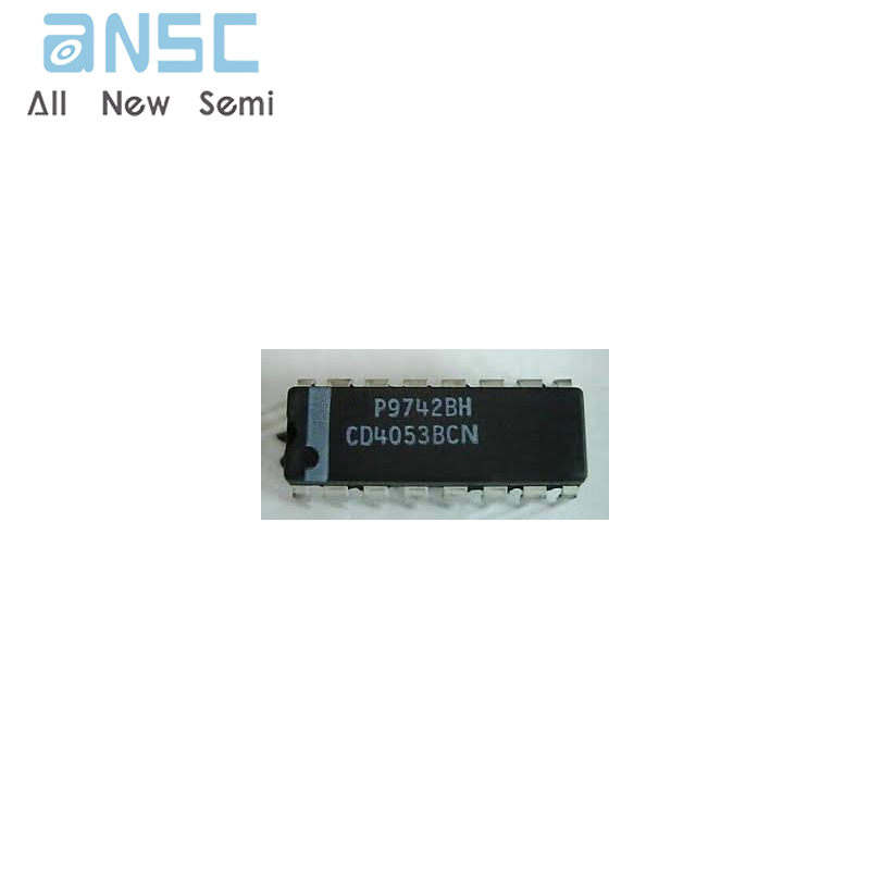
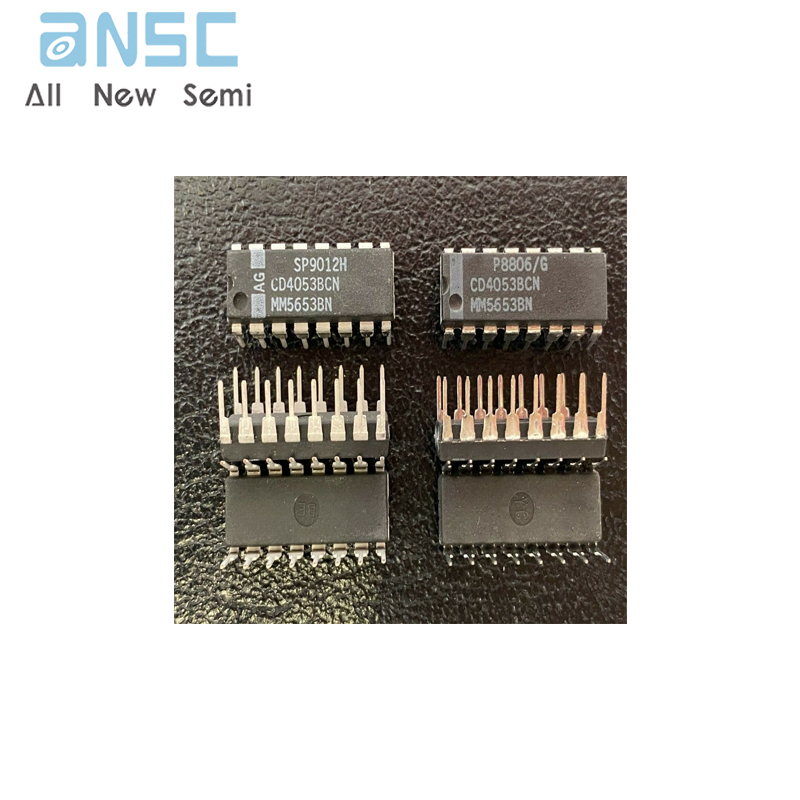
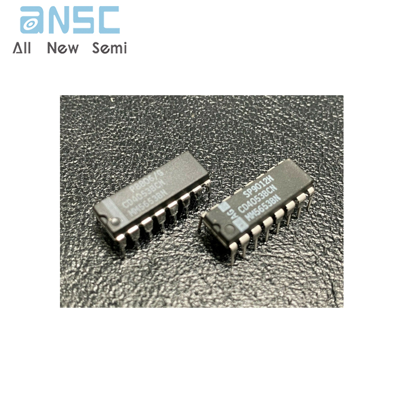
Product Photos
For more product information, please download the PDF