


Product Descriptions
The CY7C1416AV18, CY7C1427AV18, CY7C1418AV18, and CY7C1420AV18 are 1.8V Synchronous Pipelined SRAM equipped with DDR-II architecture. The DDR-II consists of an SRAM core with advanced synchronous peripheral circuitry and a 1-bit burst counter. Addresses for Read and Write are latched on alternate rising edges of the input (K) clock. Write data is registered on the rising edges of both K and K. Read data is driven on the rising edges of C and C if provided, or on the rising edge of K and K if C/C are not provided. Each address location is associated with two 8-bit words in the case of CY7C1416AV18 and two 9-bit words in the case of CY7C1427AV18 that burst sequentially into or out of the device. The burst counter always starts with a “0” internally in the case of CY7C1416AV18 and CY7C1427AV18. On CY7C1418AV18 and CY7C1420AV18, the burst counter takes in the least significant bit of the external address and bursts two 18-bit words in the case of CY7C1418AV18 and two 36-bit words in the case of CY7C1420AV18 sequentially into or out of the device.
Asynchronous inputs include impedance match (ZQ). Synchronous data outputs (Q, sharing the same physical pins as the data inputs D) are tightly matched to the two output echo clocks CQ/CQ, eliminating the need for separately capturing data from each individual DDR SRAM in the system design. Output data clocks (C/C) enable maximum system clocking and data synchronization flexibility.
All synchronous inputs pass through input registers controlled by the K or K input clocks. All data outputs pass through output registers controlled by the C or C input clocks. Writes are conducted with on-chip synchronous self-timed write circuitry.
Product Features
• 36-Mbit density (4M x 8, 4M x 9, 2M x 18, 1M x 36)
• 250-MHz clock for high bandwidth
• 2-Word burst for reducing address bus frequency
• Double Data Rate (DDR) interfaces (data transferred at 500 MHz) @ 250 MHz
• Two input clocks (K and K) for precise DDR timing
— SRAM uses rising edges only
• Two output clocks (C and C) account for clock skew and flight time mismatching
• Echo clocks (CQ and CQ) simplify data capture in high-speed systems
• Synchronous internally self-timed writes
• 1.8V core power supply with HSTL inputs and outputs
• Variable drive HSTL output buffers
• Expanded HSTL output voltage (1.4V–VDD)
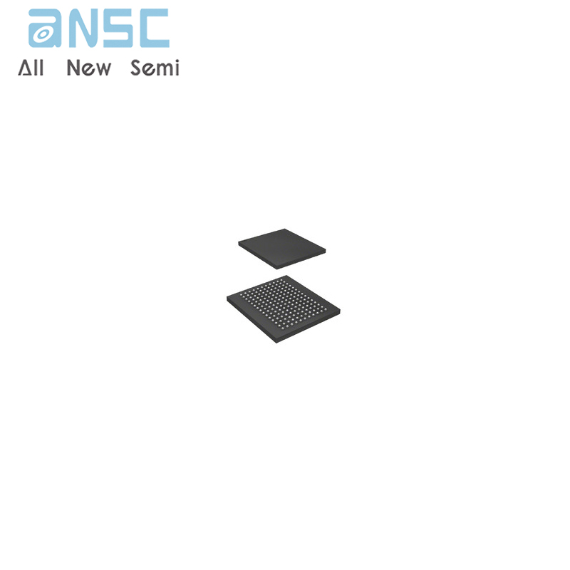
• 15 x 17 x 1.4 mm 1.0-mm pitch fBGA package, 165 ball (11x15 matrix)
• JTAG 1149.1 compatible test access port
• Delay Lock Loop (DLL) for accurate data placement
Product Specification
| Attribute | Attribute value |
| ANSM-Part# | ANSM-CY7C1418AV18-167BZC |
| Category | Integrated Circuits (ICs) |
| Memory | |
| Memory | |
| Mfr | - |
| Packaging | Tray |
| Part Status | Obsolete |
| DigiKey Programmable | Not Verified |
| Memory Type | Volatile |
| Memory Format | SRAM |
| Technology | SRAM - Synchronous, DDR II |
| Memory Size | 36Mbit |
| Memory Organization | 2M x 18 |
| Memory Interface | Parallel |
| Clock Frequency | 167 MHz |
| Voltage - Supply | 1.7V ~ 1.9V |
| Operating Temperature | 0°C ~ 70°C (TA) |
| Mounting Type | Surface Mount |
| Package / Case | 165-LBGA |
| Supplier Device Package | 165-FBGA (15x17) |
| Base Product Number | CY7C1418 |
Product Photos
For more product information, please download the PDF