



According to reports, Samsung Electronics announced its technology roadmap for chip manufacturing at its annual foundry forum held at its US chip headquarters in San Jose, California, with the aim of enhancing its competitiveness in the artificial intelligence chip foundry market through a series of upcoming technological advancements. Despite Samsung's strong position as a leading global memory chip manufacturer, it has always faced strong challenges from competitors such as TSMC in the field of wafer foundry.
According to reports, Samsung Electronics announced its technology roadmap for chip manufacturing at its annual foundry forum held at its US chip headquarters in San Jose, California, with the aim of enhancing its competitiveness in the artificial intelligence chip foundry market through a series of upcoming technological advancements. Despite Samsung's strong position as a leading global memory chip manufacturer, it has always faced strong challenges from competitors such as TSMC in the field of wafer foundry.
Samsung predicts that by 2028, its list of AI related customers will expand fivefold and revenue will increase nine times. The report pointed out that Samsung Electronics has announced a series of layouts for future artificial intelligence related chips.
In its published technology roadmap, an important innovation is the adoption of backside power supply network technology. According to Samsung, this technology has improved power, performance, and area compared to the traditional first generation 2-nanometer process, while significantly reducing voltage drop. Samsung also emphasized its comprehensive capabilities in logic, memory, and advanced packaging. Samsung believes that this will help the company win more outsourcing manufacturing orders for artificial intelligence related chips.
In addition, Samsung has also announced a Gate All Around (GAA) processor based on AI design, with the second-generation 3-nanometer GGA planned for mass production in the second half of this year and providing GAA in the upcoming 2-nanometer process. The company also confirmed that its preparation work for 1.4nm is progressing smoothly and is expected to achieve mass production by 2027.
According to the latest data from market research firm TrendForce Consulting, Samsung Foundry's revenue decreased by 7.2% to $3.36 billion in the first quarter due to the impact of the off-season of the smartphone season, as well as the shift of Android mid range smartphones and peripheral companies to domestic substitution, resulting in weak momentum in advanced processes and peripheral ICs. The market share remained at 11%.
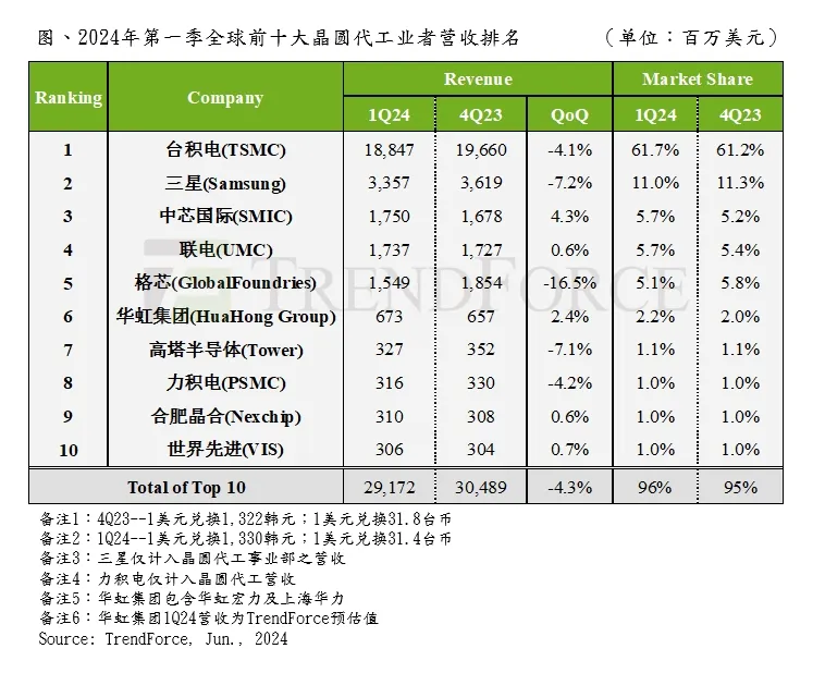
It is worth noting that despite Samsung vigorously promoting its GAA technology on forums and planning to start mass production of the second generation 3nm process in the second half of this year, Samsung executives remain silent on the progress of cooperation with key customers such as Nvidia. This also reflects to some extent that Samsung may still face significant challenges in acquiring high-end customers.
The copyright of this article belongs to the original author. The reprint of the article is only for the purpose of disseminating more information. If the author's information is marked incorrectly, please contact us immediately to modify or delete it. Thank you for your attention!