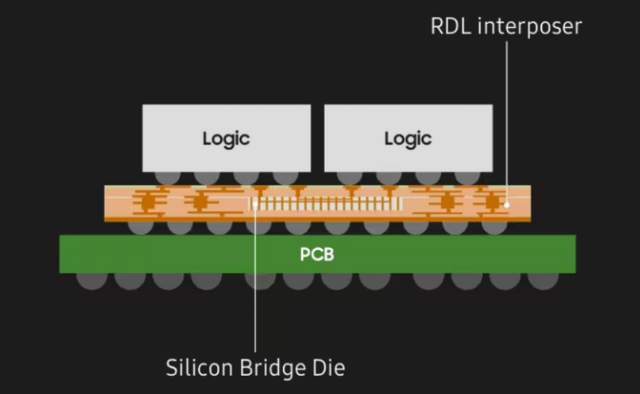
Samsung has recently introduced the next generation (2.3D) semiconductor packaging technology to strengthen its competition with Intel and TSMC, which can be used to package high-performance semiconductors such as AI chips. It is reported that this packaging technology can reduce costs by 22% without sacrificing performance.
Compared to traditional packaging technology, Samsung has used a Silicon Bridge instead of a Silicon interposer in the 2.1D packaging, thereby reducing the coverage of the entire semiconductor region.

This new design does not need to cover the entire semiconductor region, but only connects by inserting silicon bridges within the necessary areas. It is estimated that using this new packaging technology can save about 22% in cost compared to using silicon intermediate plates for packaging, without affecting performance.
It is worth mentioning that this packaging technology mainly inserts silicon bridges (embedded. E) into the rewired layer (RDL). Taking the packaging of semiconductor chips containing 12 HBMs as an example, compared to silicon intermediate boards, the cost can be reduced by 22% without reducing performance.
The copyright of this article belongs to the original author. The reprint of the article is only for the purpose of disseminating more information. If the author's information is marked incorrectly, please contact us immediately to modify or delete it. Thank you for your attention!

