Hi,welcome
86-755-88844016 +852 2632 9637 6*12 hours online call
TSMC plans to build a third factory in Japan to produce 3-nanometer chips
2023-11-22

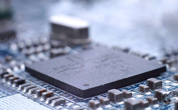
According to insiders, TSMC is considering building a third chip factory in Japan to produce advanced 3-nanometer chips; This may make Japan an important global chip manufacturing center. Insiders said that the chip foundry has informed supply chain partners that it is considering building a third factory in Kumamoto Prefecture, southern Japan, under the project code TSMC Fab-23 Phase III.


TSMC is currently building its first factory in Japan to produce chips with lower performance; According to insiders, there are also plans to build a second chip factory. It is currently unclear when the third factory will be built. The 3-nanometer chip manufacturing process is currently the most advanced commercial chip manufacturing technology, but by the time the new factory is mass-produced, the 3-nanometer process may lag behind the latest technology by 1-2 generations.

ic-  (13)_20231121143725_467


Regarding this, A TSMC spokesperson said, "We will determine our capacity expansion strategy based on customer needs, operational efficiency, government subsidies, economic conditions, etc. TSMC is committed to meeting customer needs in the long term and supporting the semiconductor industry." "We are investing to address structural changes in the manufacturing industry. We are considering the possibility of building a second factory in Japan, but currently we have no further information to disclose


The government of Japanese Prime Minister Fumio Kishida has been providing trillions of yen in subsidies to attract investment from domestic and foreign semiconductor companies. In addition to TSMC, Japan has also successfully obtained investments from Micron Technology, Samsung Electronics, and Powerchip. Japanese officials also helped domestic startup Rapidus establish a production line for cutting-edge 2nm chips in Hokkaido.


It is understood that the cost of a 3-nanometer wafer factory may be as high as $20 billion, including the machines used for production, although the specific cost will depend on when the factory is built and how to obtain land and other materials. It is currently unclear how much TSMC expects to invest in the third wafer factory. Japan usually bears about 50% of the cost of such facilities.


The copyright of this article belongs to the original author. The reprint of the article is only for the purpose of disseminating more information. If the author's information is marked incorrectly, please contact us immediately to modify or delete it. Thank you for your attention!

Hot news
Innovation breakthrough! 600 ℃ high temperature resistant memory has emerged
Recently, scientists at the University of Pennsylvania in the United States have developed a memory that can work continuously for 60 hours at a high temperature of 600 ℃. This temperature tolerance is more than twice that of current commercial storage devices, indicating that the memory has extremely strong reliability and stability, and is expected to excel in extreme environments that can cause electronic or storage device failures. It also lays the foundation for artificial intelligence systems that perform intensive computing under harsh conditions.
Samsung Electronics and Zeiss Collaborate to Strengthen Focus on EUV Technology and Semiconductor Equipment
Samsung Electronics is deepening its cooperation with Zeiss Group in next-generation EUV and chip technology. Zeiss Group is the only optical system supplier for ASML Holding NV, the world's only supplier of extreme ultraviolet (EUV) optical systems.
TSMC announces that the A16 1.6nm process is expected to be mass-produced in 2026
Recently, TSMC held the "2024 TSMC North America Technology Forum" in the United States, revealing its latest process technology, advanced packaging technology, and three-dimensional integrated circuit (3D IC) technology, using this leading semiconductor technology to drive innovation in the next generation of artificial intelligence (AI).
Samsung Electronics to Expand Silicon Valley R&D Institutions to Specially Design AI Chips
Samsung Electronics plans to expand its research and development (R&D) facility in Silicon Valley, focusing on artificial intelligence (AI) chip design. In the process of reshaping the semiconductor industry with a focus on artificial intelligence chips, Samsung aims to strengthen its design capabilities to break the current market landscape dominated by large technology companies such as Nvidia in the United States.
Storage chip prices rise, module manufacturers are unwilling to follow up
Recently, storage chip manufacturers have been insisting on raising prices, but module manufacturers have refused to purchase and are unwilling to accept price increases. According to insiders, the demand for enterprise storage and cloud data centers has remained strong, but customers in the consumer market find it difficult to bear the significant price increase.
In Q3 2023, the top 10 global semiconductor equipment manufacturers achieved revenue exceeding $25 billion, a month on month increase of 3%
According to CINNO Research statistics, the total revenue of the global semiconductor equipment manufacturer market in the third quarter of 2023 exceeded 25 billion US dollars, a year-on-year decrease of 9% and a month on month increase of 3%.
Li Jidian plans to build a factory in Japan to promote its automotive chip business
The head of Power Semiconductor Manufacturing (PSMC) recently stated that the company will use its new factory in Japan as a springboard to significantly expand its automotive semiconductor business. "Japan has huge opportunities," said Huang Chongren, CEO of Li Jidian, in a media interview. Japan has a broad market prospect and a geographical advantage where many car companies gather.
Samsung's low-priced challenge to TSMC's 2nm battle begins
According to insiders, TSMC has demonstrated the process testing results of N2 (i.e. 2 nanometers) prototypes to its major customers such as Apple and Nvidia. Samsung is also actively launching a 2-nanometer prototype and adopting a low-cost strategy to attract customers such as Nvidia.
Nikon launches a new ArF immersion lithography machine, which is 30% cheaper in price
Recently, Nikon announced that it will officially launch the ArF 193 nano immersion lithography machine "NSR-S636E" in January 2024, which will further improve production efficiency and etching accuracy. It is reported that Nikon's exposure machine adopts an enhanced iAS design, which can be used for high-precision measurement, circular warping, and distortion correction. The overlap accuracy (MMO) is higher, claiming to not exceed 2.1 nanometers.
Intel's appeal wins $2.18 billion compensation judgment overturned
The Federal Circuit Court of Appeals in the United States has announced the overturning of a 2021 ruling by a Texas court jury, which found Intel to be liable for $2.18 billion in compensation to patent technology company VLSI for patent infringement. This is one of the largest rulings in US patent history. The appellate court held that Intel's infringement of one patent involving $675 million in compensation does not constitute infringement, while the infringement of the other patent involving $1.5 billion in compensation remains valid, but the amount of compensation needs to be reconsidered by the Texas court.
User Info:
Phone number
+86
  • +86
  • +886
  • +852
Company Name
Email
Product model
Quantity
Comment message