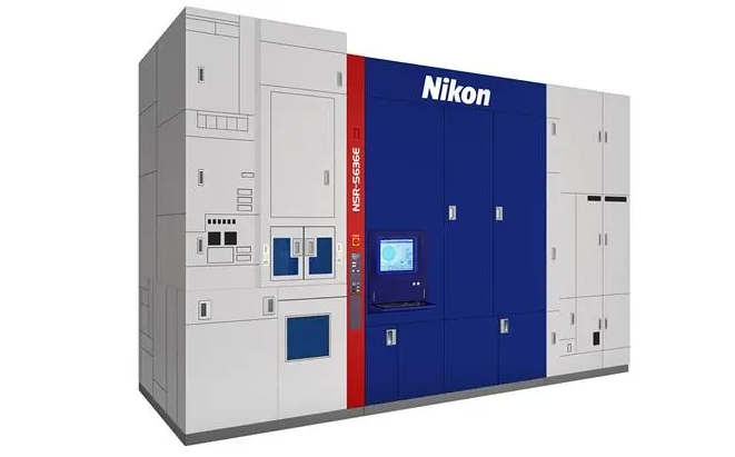
Recently, Nikon announced that it will officially launch the ArF 193 nano immersion lithography machine "NSR-S636E" in January 2024, which will further improve production efficiency and etching accuracy. It is reported that Nikon's exposure machine adopts an enhanced iAS design, which can be used for high-precision measurement, circular warping, and distortion correction. The overlap accuracy (MMO) is higher, claiming to not exceed 2.1 nanometers.
The resolution is less than 38 nanometers, the lens aperture is 1.35, and the exposure area is 26x33 millimeters.

Compared to the current model, its overall production efficiency can be improved by 10-15%, setting a new record for Nikon lithography equipment. It can produce 280 wafers per hour and has shorter downtime. Nikon also stated that, without sacrificing production efficiency, the new lithography machine can provide higher performance in semiconductor manufacturing that requires high overlap accuracy, especially in advanced logic and memory, CMOS image sensors, 3D flash memory and other 3D semiconductor manufacturing, which can be considered the best solution.
It is also understood that the light source technology of the new lithography machine is the "i-line" that has been mature since the 1990s, and with the maturity of related parts and technology, the price will be about 20-30% cheaper than competitors.
In addition to its price advantage, Nikon's ArF immersion lithography machine also has excellent reliability and maintainability. The equipment adopts advanced mechanical and electronic control systems to ensure its long-term stable operation. In addition, Nikon also provides comprehensive after-sales service and technical support to help customers solve various problems that may arise during use.
It is currently unclear how many nanometers of chips Nikon's lithography machine can produce. Many chip manufacturers have expressed their expectation that Nikon's new device can further enhance their manufacturing efficiency and capacity to meet the growing market demand. Meanwhile, some experts have pointed out that Nikon's new equipment will bring a new technological benchmark to the global semiconductor manufacturing industry, driving technological progress and development throughout the industry.
The copyright of this article belongs to the original author. The reprint of the article is only for the purpose of disseminating more information. If the author's information is marked incorrectly, please contact us immediately to modify or delete it. Thank you for your attention!

