Hi,welcome
86-755-88844016 6*12 hours online call
The semiconductor packaging material market may recover in the second half of 2023
2023-04-19

Recently, TECHCET released its latest outlook for the semiconductor packaging material market, which is expected to total approximately $26.1 billion in 2022 and reach $30 billion by 2027.


Due to the expected slowdown in the entire semiconductor industry, packaging materials are expected to decline by approximately 0.6%. However, in the second half of 2023, the market is expected to recover and achieve growth in 2024, resulting in a 5% increase in revenue for the year.
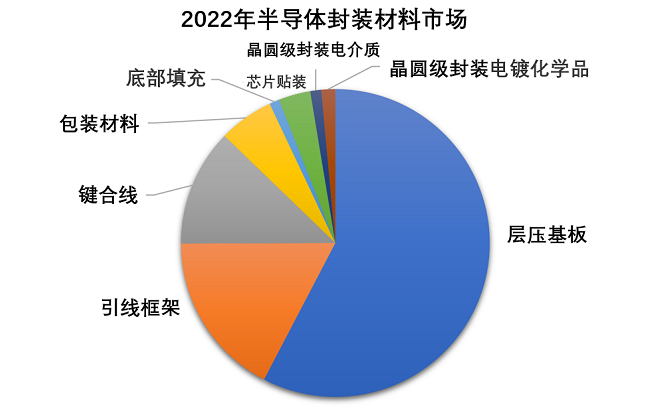
半导体材料_20230418155118_415


TECHCET stated that since 2020, packaging materials have experienced strong shipments and revenue growth. The changes in end market demand, coupled with tight supply chains and logistics constraints, have led to an increase in material prices throughout the entire supply chain. In addition, many material departments are limited in terms of available production capacity. Due to the pressure of rising costs, many suppliers have restricted investment related to production capacity. The supply chain and logistics limit the speed at which suppliers can expand their production capacity.


The upward trend in packaging material prices has completely reversed the price reduction trend of over a decade, largely due to pressure from equipment manufacturers and OSAT. Reducing costs has become a catchphrase for limiting material suppliers' investment in production capacity. These demand driven price increases have driven packaging material revenue growth of over 15% in 2020 and over 20% in 2021. As long as raw material and energy costs continue to remain high and suppliers remain cautious in their capacity expansion plans, current prices are expected to remain unchanged.


In addition, wafer level packaging, flip chip packaging, and heterogeneous integration are the main driving forces for the development of the new materials field. The biggest application of wafer level packaging is still mobile electronics, but other application scenarios, such as the automotive industry, are also growing rapidly. Flip chip interconnection is still showing strong growth in high-performance computing, high-frequency communication, and other applications, with the increasing use of copper pillar interconnection technology.


Hot news
Samsung Electronics to Expand Silicon Valley R&D Institutions to Specially Design AI Chips
Samsung Electronics plans to expand its research and development (R&D) facility in Silicon Valley, focusing on artificial intelligence (AI) chip design. In the process of reshaping the semiconductor industry with a focus on artificial intelligence chips, Samsung aims to strengthen its design capabilities to break the current market landscape dominated by large technology companies such as Nvidia in the United States.
Storage chip prices rise, module manufacturers are unwilling to follow up
Recently, storage chip manufacturers have been insisting on raising prices, but module manufacturers have refused to purchase and are unwilling to accept price increases. According to insiders, the demand for enterprise storage and cloud data centers has remained strong, but customers in the consumer market find it difficult to bear the significant price increase.
In Q3 2023, the top 10 global semiconductor equipment manufacturers achieved revenue exceeding $25 billion, a month on month increase of 3%
According to CINNO Research statistics, the total revenue of the global semiconductor equipment manufacturer market in the third quarter of 2023 exceeded 25 billion US dollars, a year-on-year decrease of 9% and a month on month increase of 3%.
Li Jidian plans to build a factory in Japan to promote its automotive chip business
The head of Power Semiconductor Manufacturing (PSMC) recently stated that the company will use its new factory in Japan as a springboard to significantly expand its automotive semiconductor business. "Japan has huge opportunities," said Huang Chongren, CEO of Li Jidian, in a media interview. Japan has a broad market prospect and a geographical advantage where many car companies gather.
Samsung's low-priced challenge to TSMC's 2nm battle begins
According to insiders, TSMC has demonstrated the process testing results of N2 (i.e. 2 nanometers) prototypes to its major customers such as Apple and Nvidia. Samsung is also actively launching a 2-nanometer prototype and adopting a low-cost strategy to attract customers such as Nvidia.
Nikon launches a new ArF immersion lithography machine, which is 30% cheaper in price
Recently, Nikon announced that it will officially launch the ArF 193 nano immersion lithography machine "NSR-S636E" in January 2024, which will further improve production efficiency and etching accuracy. It is reported that Nikon's exposure machine adopts an enhanced iAS design, which can be used for high-precision measurement, circular warping, and distortion correction. The overlap accuracy (MMO) is higher, claiming to not exceed 2.1 nanometers.
Intel's appeal wins $2.18 billion compensation judgment overturned
The Federal Circuit Court of Appeals in the United States has announced the overturning of a 2021 ruling by a Texas court jury, which found Intel to be liable for $2.18 billion in compensation to patent technology company VLSI for patent infringement. This is one of the largest rulings in US patent history. The appellate court held that Intel's infringement of one patent involving $675 million in compensation does not constitute infringement, while the infringement of the other patent involving $1.5 billion in compensation remains valid, but the amount of compensation needs to be reconsidered by the Texas court.
Spend 5 billion euros! STMicroelectronics will build a new SiC wafer factory
Recently, STMicroelectronics has decided to further expand its production facilities by establishing a brand new silicon carbide (SiC) semiconductor wafer fab in Catane, Sicily, Italy. The total investment amount is up to 5 billion euros, and the wafer factory will specialize in producing silicon carbide chips, which are key technologies for electric vehicles and have strong growth potential.
AMD plans to establish the world's largest design center in India
AMD announced the opening of its largest global design center, AMD Technostar, in Bangalore, India. This move is also part of AMD's global expansion, aimed at enhancing its competitiveness in the fiercely competitive semiconductor market.
Apple may abandon independent research and development of 5G modem chips
Supply chain sources have revealed that Apple may decide to stop developing its self-developed 5G modem chip after multiple failed attempts to improve it.
User Info:
Phone number
+86
  • +86
  • +886
  • +852
Company Name
Email
Product model
Quantity
Comment message