

Hi,welcome
+86 135 5637 6665 +852 2632 9637 6*12 hours online call
Meiguang Launches 8-Layer Stacked 24GB Capacity Second Generation HBM3 with 2.5x Improved Memory Performance
2023-07-29

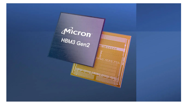
Recently, Micron Technology announced that it has begun to send samples of its first 8-high 24GB HBM3 Gen2 memory product, with bandwidth greater than 1.2TB/s and pin speed greater than 9.2Gb/s, which is 50% higher than the current HBM3 solution, and its performance per watt is 2.5 times higher than previous generations of products.
未标题-1

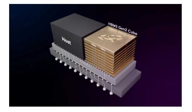
It is reported that Micron Technology HBM solution adopts 1 β (1-beta) DRAM process node, which allows the assembly of 24Gb DRAM chips into 8-high cubes within industry standard packaging sizes. In addition, Meguiar's 36GB capacity product with 12 layers of stacking will also begin sampling in the first quarter of 2024. Compared with existing competitive solutions, Micron Technology provides 50% more capacity at a given stack height. The improvement in performance to power ratio and pin speed of Meguiar's second-generation HBM3 products is crucial for managing the extreme power demands of today's AI data centers. Meguiar has achieved significant improvement in energy efficiency through technological innovation. For example, compared with other HBM3 solutions in the industry, Meguiar doubled the number of silicon through holes (TSVs), increased metal density by five times to reduce thermal resistance, and designed more energy-efficient Datapath.


Micron Technology said that as part of the development of HBM3 Gen2 products, the cooperation between Micron Technology and TSMC laid the foundation for the smooth introduction and integration of computing systems designed and applied by AI and HPC. TSMC has received samples of Micron Technology's HBM3 Gen2 memory, and is working closely with Micron Technology for further evaluation and testing to help customers innovate in next-generation High-performance computing applications.

未标题-2


Praveen Vaidyanathan, Vice President of Micron and General Manager of the Computing Products Business Group of the Computing and Network Business Unit, said, "Micron's second generation HBM3 solution is designed to provide customers and the industry with excellent AI and High-performance computing solutions. One of our important criteria is whether the product is easy to integrate on the customer's platform. Micron's HBM3 has a fully programmable memory Built-in self-test (MBIST) The function can run at full specification pin speeds, enabling Meiguang to provide customers with stronger testing capabilities, achieve efficient collaboration, and help customers shorten product launch time


Previously, Micron Technology launched a α The 96GB DDR5 module with a (1-alpha) 24Gb single chip DRAM chip is designed for server solutions with high capacity requirements. This launch is based on 1 β 24GB HBM3 product with 24Gb chips. Micron Technology plans to launch in the first half of 2024 based on 1 β 128GB DDR5 module with 32Gb single chip DRAM chip.

Hot news
Differences in the Performance of LED Core Technologies
The core performance indicators of LED devices are mainly reflected in the following six aspects
PCB wiring principles and techniques
1、 Manually wiring as much as possible
Mikroe Motion 2 Click Board Product Introduction
Mikroe Motion 2 Click is based on the Panasonic EKMC1607112 PIR motion sensor and is used as a human motion detector
SK Hynix develops a new generation of mobile NAND flash memory solutions
As the industry's highest-performance product, it will begin mass production in the third quarter of this year and be integrated into edge-side AI smartphones
Samsung is about to mass produce Galaxy Tab S10
According to media reports, Samsung is about to launch a new generation of Galaxy Tab S10 series, which is testing the Galaxy Tab S10+equipped with MediaTek Dimensity 9300+, changing the previous strategy of Qualcomm Snapdragon chip monopoly.
Samsung announces chip manufacturing technology roadmap
According to reports, Samsung Electronics announced its technology roadmap for chip manufacturing at its annual foundry forum held at its US chip headquarters in San Jose, California, with the aim of enhancing its competitiveness in the artificial intelligence chip foundry market through a series of upcoming technological advancements. Despite Samsung's strong position as a leading global memory chip manufacturer, it has always faced strong challenges from competitors such as TSMC in the field of wafer foundry.
NXP and World Advanced Plan Invest $7.8 billion in Singapore to Build a Wafer Factory
On June 5th, World Advanced and NXP Semiconductors announced plans to jointly establish the VisionPower Semiconductor Manufacturing Company (VSMC) joint venture in Singapore to build a 12 inch (300mm) wafer fab. The wafer factory has an investment of approximately 7.8 billion US dollars, with World Advanced investing 2.4 billion US dollars to hold 60% equity, and NXP investing 1.6 billion US dollars to hold 40% equity.
Mitsubishi Electric Kumamoto Prefecture SiC Wafer Factory to Start Production Ahead of Time
Recently, Mitsubishi Electric announced at a performance briefing that its SiC wafer plant located in Kumamoto Prefecture will be put into operation ahead of schedule due to strong market demand. The factory, originally scheduled to start operation in April 2026, will be put into production in November 2025, about 5 months ahead of schedule.
Passive component leader National Giant plans to transform into IDM company
In the past 5 to 10 years, Guoju has been steadily developing, consciously investing in new corporate groups through mergers and private equity investments.
Intel, Microsoft, Broadcom and other eight giants jointly launch the UALink standard
According to reports, Intel, Google, Microsoft, Meta, and other tech giants have announced the establishment of a new industry organization called "Ultra Accelerator Link (UALink) Promotion Group".
User Info:
Phone number
+86
  • +86
  • +886
  • +852
Company Name
Email
Product model
Quantity
Comment message