



Nexperia, a manufacturer in the field of basic semiconductor devices, recently announced the launch of a new 500 mA dual channel built-in resistance transistor (RET) series of products, all in ultra compact DFN 2020 (D) -6 packaging. The new series of devices are suitable for load switches in wearable devices and smartphones, as well as for digital circuits with higher power requirements. For example, space limited computing, communication, industrial, and automotive applications. It is worth noting that the RET packaged with DFN adopts a dual space saving scheme, which can double the space utilization efficiency. Firstly, by cleverly integrating bipolar transistors (BJTs) and resistors into a single package, a significant amount of circuit board space can be saved. In addition, the leadless DFN packaging itself has higher spatial efficiency. This strategy of effective integration and packaging fully highlights Nexperia's unremitting efforts to meet the compact space requirements of contemporary electronic devices.
In order to reduce the number of components and simplify circuit board design, 12 new RETs combine dual channel BJTs with bias resistors in the same package. Simultaneously, a second integrated resistor is connected in parallel on the base emitter path to create a voltage divider for setting the base voltage. Furthermore, it can achieve finer fine-tuning and better shut-off characteristics. Due to the higher tolerance of these internal resistors compared to external resistors, RET is suitable for switch applications where transistors operate in either on or off states and helps overcome the temperature dependence of standard BJTs. In addition, it can also reduce the costs associated with patches and manual processing.
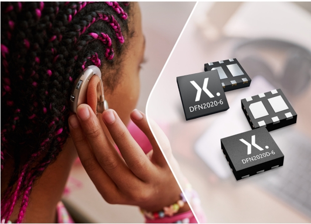
This series of RET devices offers dual NPN/NPN, NPN/PNP, and PNP/PNP options. Unlike similar competing devices, Nexperia RET's miniature DFN2020 (D) -6 package size is only 2 mm x 2 mm x 0.65 mm, which can fully provide its specified 500 mA output current. This package is specifically designed to achieve excellent thermal performance in high-power applications, providing a total output power of up to 1 W at collector emitter voltage (VCEO, base open circuit) of up to 50 V.
Nexperia RET devices are available in both standard and vehicle level (AEC-Q101 compliant) versions. This product portfolio includes over 400 products, including single channel and dual channel RETs, as well as a wide range of resistor combinations. The Nexperia RET series products offer DFN and pin based SMD packaging, which can meet the diverse needs of many applications.
About Nexperia
Nexperia, headquartered in the Netherlands, is a global semiconductor company with a rich and long history of development in Europe. Currently, it has more than 15000 employees in Europe, Asia, and the United States. As a leader in the development and production of basic semiconductor devices, Nexperia's devices are widely used in various application fields such as automotive, industrial, mobile, and consumer, providing support for almost all the basic functions of electronic design in the world.
Nexperia provides services to customers worldwide, with annual product shipments exceeding 100 billion units. These products have become industry benchmarks in terms of efficiency (such as process, size, power, and performance) and are widely recognized. Nexperia has a rich IP product portfolio and continuously expanding product range, and has been certified to IATF 16949, ISO 9001, ISO 14001, and ISO 45001 standards, fully demonstrating the company's firm commitment to innovation, efficiency, sustainable development, and meeting the strict requirements of the industry. Nexperia dual channel 500 mA RET enables high-power load switching
The copyright of this article belongs to the original author. The reprint of the article is only for the purpose of disseminating more information. If the author's information is marked incorrectly, please contact us immediately to modify or delete it. Thank you for your attention!