Hi,welcome
86-755-88844016 +852 2632 9637 6*12 hours online call
Samsung plans to launch 3D AI chip packaging "SAINT" in 2024
2023-11-17

As semiconductor microfabrication processes approach the physical limit, advanced packaging technology has become the focus of competition. TSMC is the first to launch the 3Dfabric platform, and Samsung plans to launch the "SAINT" advanced 3D chip packaging technology to catch up.


It is reported that Samsung plans to launch advanced 3D chip packaging technology SAINT (Samsung Advanced Interconnection Technology) in 2024, which can integrate the memory and processor of high-performance chips such as AI chips in a smaller size package. Samsung SAINT will be used to develop various solutions, offering three types of packaging technologies. Samsung has passed validation testing, but plans to expand its service scope later next year after further testing with customers, with the goal of improving the performance of data center AI chips and built-in AI function mobile application processors.
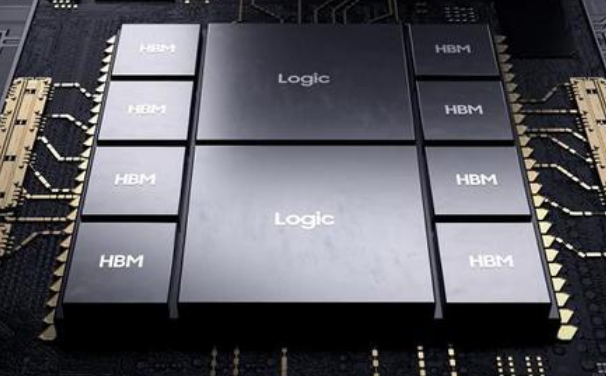

三星_20231116145726_604


The demand for generative AI applications such as ChatGPT has driven the growth of the semiconductor market that can quickly process large amounts of data, thereby promoting the rapid development of advanced packaging technology. According to research firm Yole Intelligence, the global advanced chip packaging market will grow from $44.3 billion in 2022 to $66 billion in 2027. Among them, 3D packaging is expected to account for about 25% of the market share, which is about $15 billion in market size. This number is eye-catching and has also driven the vigorous development of 3D packaging technology.


Other companies such as TSMC are investing heavily in testing and upgrading their own 3D chip to chip stack technology "SoIC" to meet the needs of customers such as Apple and Nvidia. Lianhua Electronics is also launching the W2W 3D IC project, and as for Intel, it is starting to manufacture advanced chips using its own new generation 3D chip packaging technology "Fooveros". It is expected that the advanced chip packaging market will grow rapidly in the next few years, with 3D packaging accounting for approximately 25% of the market share.


The copyright of this article belongs to the original author. The reprint of the article is only for the purpose of disseminating more information. If the author's information is marked incorrectly, please contact us immediately to modify or delete it. Thank you for your attention!

Hot news
Samsung Electronics and Zeiss Collaborate to Strengthen Focus on EUV Technology and Semiconductor Equipment
Samsung Electronics is deepening its cooperation with Zeiss Group in next-generation EUV and chip technology. Zeiss Group is the only optical system supplier for ASML Holding NV, the world's only supplier of extreme ultraviolet (EUV) optical systems.
TSMC announces that the A16 1.6nm process is expected to be mass-produced in 2026
Recently, TSMC held the "2024 TSMC North America Technology Forum" in the United States, revealing its latest process technology, advanced packaging technology, and three-dimensional integrated circuit (3D IC) technology, using this leading semiconductor technology to drive innovation in the next generation of artificial intelligence (AI).
Samsung Electronics to Expand Silicon Valley R&D Institutions to Specially Design AI Chips
Samsung Electronics plans to expand its research and development (R&D) facility in Silicon Valley, focusing on artificial intelligence (AI) chip design. In the process of reshaping the semiconductor industry with a focus on artificial intelligence chips, Samsung aims to strengthen its design capabilities to break the current market landscape dominated by large technology companies such as Nvidia in the United States.
Storage chip prices rise, module manufacturers are unwilling to follow up
Recently, storage chip manufacturers have been insisting on raising prices, but module manufacturers have refused to purchase and are unwilling to accept price increases. According to insiders, the demand for enterprise storage and cloud data centers has remained strong, but customers in the consumer market find it difficult to bear the significant price increase.
In Q3 2023, the top 10 global semiconductor equipment manufacturers achieved revenue exceeding $25 billion, a month on month increase of 3%
According to CINNO Research statistics, the total revenue of the global semiconductor equipment manufacturer market in the third quarter of 2023 exceeded 25 billion US dollars, a year-on-year decrease of 9% and a month on month increase of 3%.
Li Jidian plans to build a factory in Japan to promote its automotive chip business
The head of Power Semiconductor Manufacturing (PSMC) recently stated that the company will use its new factory in Japan as a springboard to significantly expand its automotive semiconductor business. "Japan has huge opportunities," said Huang Chongren, CEO of Li Jidian, in a media interview. Japan has a broad market prospect and a geographical advantage where many car companies gather.
Samsung's low-priced challenge to TSMC's 2nm battle begins
According to insiders, TSMC has demonstrated the process testing results of N2 (i.e. 2 nanometers) prototypes to its major customers such as Apple and Nvidia. Samsung is also actively launching a 2-nanometer prototype and adopting a low-cost strategy to attract customers such as Nvidia.
Nikon launches a new ArF immersion lithography machine, which is 30% cheaper in price
Recently, Nikon announced that it will officially launch the ArF 193 nano immersion lithography machine "NSR-S636E" in January 2024, which will further improve production efficiency and etching accuracy. It is reported that Nikon's exposure machine adopts an enhanced iAS design, which can be used for high-precision measurement, circular warping, and distortion correction. The overlap accuracy (MMO) is higher, claiming to not exceed 2.1 nanometers.
Intel's appeal wins $2.18 billion compensation judgment overturned
The Federal Circuit Court of Appeals in the United States has announced the overturning of a 2021 ruling by a Texas court jury, which found Intel to be liable for $2.18 billion in compensation to patent technology company VLSI for patent infringement. This is one of the largest rulings in US patent history. The appellate court held that Intel's infringement of one patent involving $675 million in compensation does not constitute infringement, while the infringement of the other patent involving $1.5 billion in compensation remains valid, but the amount of compensation needs to be reconsidered by the Texas court.
Spend 5 billion euros! STMicroelectronics will build a new SiC wafer factory
Recently, STMicroelectronics has decided to further expand its production facilities by establishing a brand new silicon carbide (SiC) semiconductor wafer fab in Catane, Sicily, Italy. The total investment amount is up to 5 billion euros, and the wafer factory will specialize in producing silicon carbide chips, which are key technologies for electric vehicles and have strong growth potential.
User Info:
Phone number
+86
  • +86
  • +886
  • +852
Company Name
Email
Product model
Quantity
Comment message