Hi,welcome
86-755-88844016 +852 2632 9637 6*12 hours online call
Samsung Electronics CIS products have seen a maximum price increase of 30%
2023-12-01

After a long period of downturn, the consumer electronics industry has finally ushered in the dawn of recovery. Recently, media reports have reported that Samsung Electronics has issued a CIS price increase notice to customers, with an average increase of up to 25% in the first quarter of next year, and some products have seen the highest increase of up to 30%. The price increase mainly focuses on products with specifications above 32 million pixels.


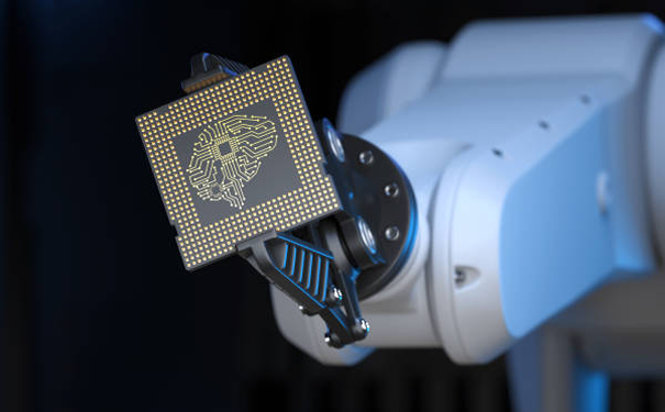
According to data, CIS, also known as Contact Image Sensor, is the core component of camera modules and is widely used in fields such as mobile phones, consumers, computers, security, automobiles, and industry. Among them, mobile phones are the largest end-user market for CIS.
ic-  (8)_20231130154308_635


At present, there are a total of 52 ISOCELL image sensor models listed on Samsung's official website. This includes familiar models such as GN5, GN2, JN1, HP2, HP3, etc. Earlier this month, Samsung also released a 50 megapixel ISOCELL GNK camera sensor, which integrates dual pixel technology and advanced HDR technology, and has a size of 1/1.3 inches and a pixel size of 1.2 micrometers.


In recent years, with the increasing penetration rate of the new energy vehicle and intelligent vehicle markets, the demand for automotive semiconductors has skyrocketed, and the demand for CIS is also the same.


The industry has revealed that a L2 car requires approximately 8-12 CIS cars. Compared to consumer grade CIS cars, in car CIS cars are relatively less price sensitive. Under the same performance, in car CIS cars are more expensive and have a larger value space. At the same time, as cars continue to move towards intelligence and autonomous driving, "vision" has become a crucial step, which will also make automotive CIS very useful in the future.


The copyright of this article belongs to the original author. The reprint of the article is only for the purpose of disseminating more information. If the author's information is marked incorrectly, please contact us immediately to modify or delete it. Thank you for your attention!

Hot news
TSMC announces that the A16 1.6nm process is expected to be mass-produced in 2026
Recently, TSMC held the "2024 TSMC North America Technology Forum" in the United States, revealing its latest process technology, advanced packaging technology, and three-dimensional integrated circuit (3D IC) technology, using this leading semiconductor technology to drive innovation in the next generation of artificial intelligence (AI).
Samsung Electronics to Expand Silicon Valley R&D Institutions to Specially Design AI Chips
Samsung Electronics plans to expand its research and development (R&D) facility in Silicon Valley, focusing on artificial intelligence (AI) chip design. In the process of reshaping the semiconductor industry with a focus on artificial intelligence chips, Samsung aims to strengthen its design capabilities to break the current market landscape dominated by large technology companies such as Nvidia in the United States.
Storage chip prices rise, module manufacturers are unwilling to follow up
Recently, storage chip manufacturers have been insisting on raising prices, but module manufacturers have refused to purchase and are unwilling to accept price increases. According to insiders, the demand for enterprise storage and cloud data centers has remained strong, but customers in the consumer market find it difficult to bear the significant price increase.
In Q3 2023, the top 10 global semiconductor equipment manufacturers achieved revenue exceeding $25 billion, a month on month increase of 3%
According to CINNO Research statistics, the total revenue of the global semiconductor equipment manufacturer market in the third quarter of 2023 exceeded 25 billion US dollars, a year-on-year decrease of 9% and a month on month increase of 3%.
Li Jidian plans to build a factory in Japan to promote its automotive chip business
The head of Power Semiconductor Manufacturing (PSMC) recently stated that the company will use its new factory in Japan as a springboard to significantly expand its automotive semiconductor business. "Japan has huge opportunities," said Huang Chongren, CEO of Li Jidian, in a media interview. Japan has a broad market prospect and a geographical advantage where many car companies gather.
Samsung's low-priced challenge to TSMC's 2nm battle begins
According to insiders, TSMC has demonstrated the process testing results of N2 (i.e. 2 nanometers) prototypes to its major customers such as Apple and Nvidia. Samsung is also actively launching a 2-nanometer prototype and adopting a low-cost strategy to attract customers such as Nvidia.
Nikon launches a new ArF immersion lithography machine, which is 30% cheaper in price
Recently, Nikon announced that it will officially launch the ArF 193 nano immersion lithography machine "NSR-S636E" in January 2024, which will further improve production efficiency and etching accuracy. It is reported that Nikon's exposure machine adopts an enhanced iAS design, which can be used for high-precision measurement, circular warping, and distortion correction. The overlap accuracy (MMO) is higher, claiming to not exceed 2.1 nanometers.
Intel's appeal wins $2.18 billion compensation judgment overturned
The Federal Circuit Court of Appeals in the United States has announced the overturning of a 2021 ruling by a Texas court jury, which found Intel to be liable for $2.18 billion in compensation to patent technology company VLSI for patent infringement. This is one of the largest rulings in US patent history. The appellate court held that Intel's infringement of one patent involving $675 million in compensation does not constitute infringement, while the infringement of the other patent involving $1.5 billion in compensation remains valid, but the amount of compensation needs to be reconsidered by the Texas court.
Spend 5 billion euros! STMicroelectronics will build a new SiC wafer factory
Recently, STMicroelectronics has decided to further expand its production facilities by establishing a brand new silicon carbide (SiC) semiconductor wafer fab in Catane, Sicily, Italy. The total investment amount is up to 5 billion euros, and the wafer factory will specialize in producing silicon carbide chips, which are key technologies for electric vehicles and have strong growth potential.
AMD plans to establish the world's largest design center in India
AMD announced the opening of its largest global design center, AMD Technostar, in Bangalore, India. This move is also part of AMD's global expansion, aimed at enhancing its competitiveness in the fiercely competitive semiconductor market.
User Info:
Phone number
+86
  • +86
  • +886
  • +852
Company Name
Email
Product model
Quantity
Comment message