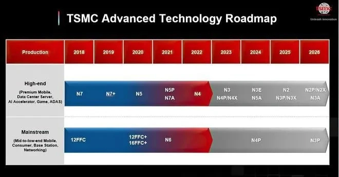
TSMC recently held a technical seminar, stating that its 3nm process node has entered the right track, and the N3P node will be put into mass production in the second half of 2024.
N3P is based on N3E process nodes to further improve energy efficiency and transistor density. TSMC stated that the yield of N3E nodes has been further improved, which is comparable to the mature 5nm process.

It is reported that TSMC executives have stated that the N3P process has completed quality verification, and its yield rate can be close to N3E. As an optical miniaturization process, N3P is compatible with N3E in terms of IP modules, design rules, EDA tools and methods, so TSMC stated that the entire transition process was very smooth.
The key advantage of N3P lies in its enhanced specifications. Compared to N3E, chip designers can expect a performance improvement of about 4% at the same power consumption, or a power reduction of about 9% at matched clocks. For typical chip designs composed of logic, SRAM, and analog components, the transistor density has also increased by 4%.
The copyright of this article belongs to the original author. The reprint of the article is only for the purpose of disseminating more information. If the author's information is marked incorrectly, please contact us immediately to modify or delete it. Thank you for your attention!

