



As the industry's top-performing product, it will enter mass production in the third quarter of this year and be equipped in edge-side AI smartphones.
Compared to the previous generation product, there has been significant improvement in performance degradation due to prolonged use, with its service life also increasing by 40 percent.
"Following HBM, it also leads the AI-oriented memory market in NAND flash solutions."
On May 9, 2024, SK Hynix announced the development of a mobile NAND flash memory solution product, "ZUFS (Zoned UFS) 4.0," designed for On-Device AI*.
SK Hynix stated, "ZUFS 4.0 is a next-generation mobile NAND flash solution designed for edge AI smartphones, delivering industry-leading performance." The company further emphasized, "With this product, following the ultra-high-performance DRAM including HBM, SK Hynix will lead the AI-oriented memory market in the NAND flash sector."
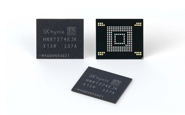
ZUFS distinguishes and manages data generated by smartphone applications based on their respective characteristics. Unlike the existing UFS method of mixed storage without dividing regions, ZUFS can store data with different purposes and usage frequencies in zones, improving the running speed of mobile operating systems and the data management efficiency of storage devices.
As a result, ZUFS has improved the running time of mobile applications by about 45% compared to existing UFS in long-term usage environments. Moreover, ZUFS has achieved a more than 4-fold improvement in storage read and write performance, thereby increasing the product's lifespan by approximately 40 percent.
The company has long predicted that the market demand for high-performance NAND flash memory solutions is expected to occur, and has been collaborating with global platform enterprises to develop ZUFS since 2019 before the AI boom.
SK Hynix provides customers with initial trial products, and based on these product specifications, collaborates with customers to develop 4.0 products that comply with JEDEC * standards. The company will begin mass production of ZUFS 4.0 products in the third quarter of this year, and its products will be equipped with end-to-end AI smartphones launched by global mobile phone companies.
An Xuan, Vice President of SK Hynix NAND Flash Solutions Committee (N-S Committee), said, "As technology giants focus on developing end side devices equipped with self-developed generative AI, the performance requirements for the required memory are increasingly increasing. The company will timely supply high-performance NAND flash memory solutions that meet customer requirements, while strengthening partnerships with leading global ICT companies to consolidate its position as the 'world's top AI oriented memory supplier'. ”
*On Device AI: Implementing artificial intelligence on the device itself, rather than relying on physically separated servers for computation. Due to the self collection of information and computation by terminal devices such as smartphones or PCs, the response speed of AI functions can be improved and user customized AI service functions can be enhanced.
** ZUFS(Zoned Universal Flash Storage): A new product that improves data management efficiency based on Universal Flash Storage (UFS) applicable to electronic products such as digital cameras and mobile phones. Its products effectively manage data by storing data with similar characteristics in the same zone, thereby optimizing data transfer between the operating system and storage.
*JEDEC (Joint Electron Device Engineering Council) is an international semiconductor device standards organization that determines specifications for semiconductors.
What is the equivalent component for [model]
What is a [brand] [parts series] in stock
What are the key specifications of [model]
What is the lead time for [specific component]
What is the best alternative to [discontinued model]
What is the difference between [Component A] and [Component B]
What is the function of [specific IC] in [Application]