

Hi,welcome
+86 135 5637 6665 +852 2632 9637 6*12 hours online call
PCB wiring principles and techniques
2026-05-23

1、 Manually wiring as much as possible


Generally speaking, PCB design software includes the function of automatic routing, but in reality, no automatic routing can completely replace the skills, experience, and flexibility of PCB layout engineers. (Manually give a thumbs up to the PCB Layout engineer)


In some cases, you can use automatic routing:


  • After placing all the components, you can use automatic routing to check your completion rate. If it is below 85%, you need to adjust the placement of your components.


  • During wiring, bottlenecks and other critical connection points may detach from cracks and can be identified using automatic routing functionality.


  • When you don't know how to start wiring or encounter difficulties, you can use automatic wiring as a source of inspiration.


In summary, wiring is both a science and an art, and it is recommended to manually route as much as possible to ensure accuracy and reliability.


2、 Understand the manufacturer's specifications


When you start laying copper traces, take the time to ask your manufacturer if they have requirements for minimum trace width, trace spacing, and the number of PCB layers they can assemble.


By understanding this information in advance, you can set the routing width and spacing values in the design rules to avoid rewiring the entire PCB layout.


3、 Choose the appropriate wiring width


The geometric shape (thickness and width) of the wiring ensures that the circuit operates normally under all environmental and load conditions. The wiring of PCBs is used to transmit electrical signals, so it must have a width compatible with the current passing through them.


PCB layout engineers must determine the minimum width of each trace to avoid the risk of overheating of the circuit board; This parameter directly affects the wiring process as it reduces the available space on the PCB.


If available space is not a problem, it is recommended to use wiring with a width greater than the minimum value to improve the thermal management and reliability of the circuit board. The wiring on the outer layer can achieve better heat exchange, so it may have a smaller width.
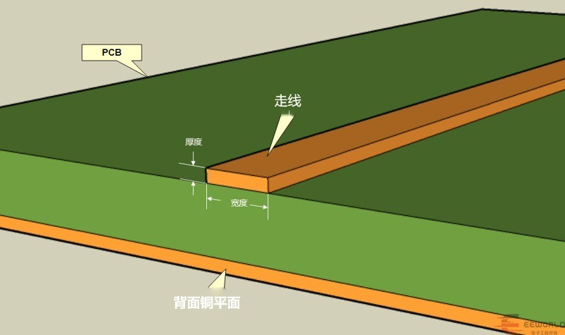

未标题-1

Line width


4、 Leave enough space between the wiring and solder pads


It is crucial to leave sufficient space between PCB routing and solder pads (as shown below) to avoid short circuits during PCB manufacturing or assembly stages.


Generally speaking, it is recommended to leave appropriate gaps between each adjacent wire and pad, and there must always be sufficient space around them without wires or pads to avoid the risk of electric shock.
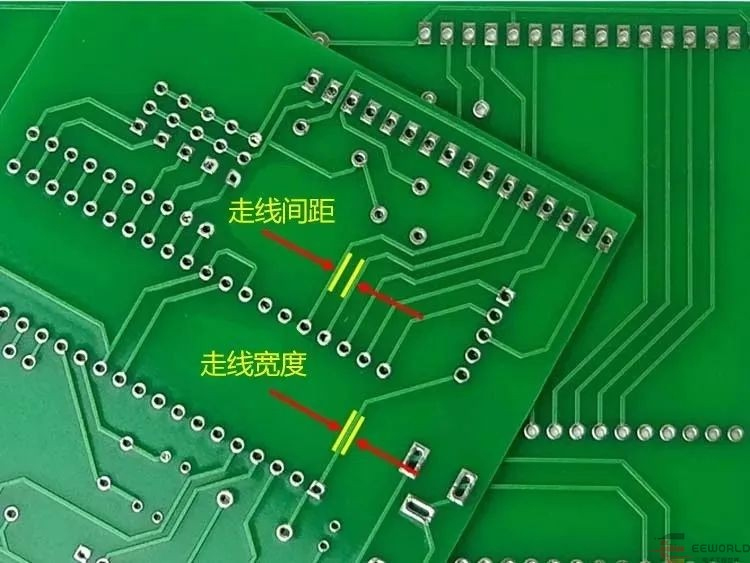

未标题-2

Distance and thickness of wiring


5、 PCB component placement


The placement of components determines the success of PCB design. To properly place components, it is necessary to fully understand their characteristics.


For example, thermal electrolytic capacitors must be kept away from heating diodes, resistors, and inductors.


Here are some simple rules of thumb:


  • Attention must be paid to components with multiple pins, as these components occupy a significant amount of space.


  • Keep components placed in the same direction


  • Consider the functionality of each component and its relationship with other components before placement.


  • If the components have already been purchased, it is recommended to print the layout on paper according to the size and check if the components are suitable.
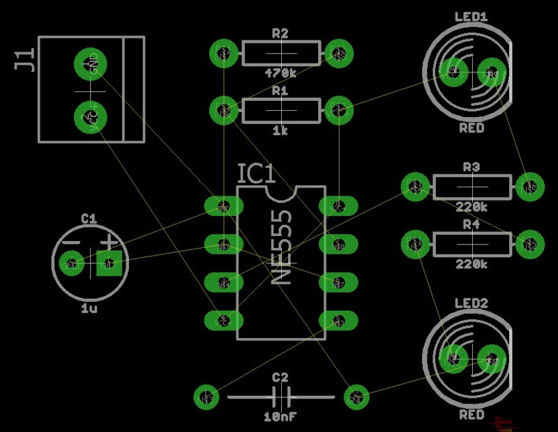

未标题-3

PCB component placement diagram


So come and give it a try~


How to identify genuine vs fake components 

How to choose the right capacitor for [application scenario]

How to solder [Micro package model] components 

How to check the traceability of [brand] semiconductors 

How to optimize PCB design to reduce component cost

How to manage long lead time components in inventory

How to implement RoHS compliance in electronic components


Click to get:

https://allnewsemi.com


Hot news
Differences in the Performance of LED Core Technologies
The core performance indicators of LED devices are mainly reflected in the following six aspects
Mikroe Motion 2 Click Board Product Introduction
Mikroe Motion 2 Click is based on the Panasonic EKMC1607112 PIR motion sensor and is used as a human motion detector
SK Hynix develops a new generation of mobile NAND flash memory solutions
As the industry's highest-performance product, it will begin mass production in the third quarter of this year and be integrated into edge-side AI smartphones
Samsung is about to mass produce Galaxy Tab S10
According to media reports, Samsung is about to launch a new generation of Galaxy Tab S10 series, which is testing the Galaxy Tab S10+equipped with MediaTek Dimensity 9300+, changing the previous strategy of Qualcomm Snapdragon chip monopoly.
Samsung announces chip manufacturing technology roadmap
According to reports, Samsung Electronics announced its technology roadmap for chip manufacturing at its annual foundry forum held at its US chip headquarters in San Jose, California, with the aim of enhancing its competitiveness in the artificial intelligence chip foundry market through a series of upcoming technological advancements. Despite Samsung's strong position as a leading global memory chip manufacturer, it has always faced strong challenges from competitors such as TSMC in the field of wafer foundry.
NXP and World Advanced Plan Invest $7.8 billion in Singapore to Build a Wafer Factory
On June 5th, World Advanced and NXP Semiconductors announced plans to jointly establish the VisionPower Semiconductor Manufacturing Company (VSMC) joint venture in Singapore to build a 12 inch (300mm) wafer fab. The wafer factory has an investment of approximately 7.8 billion US dollars, with World Advanced investing 2.4 billion US dollars to hold 60% equity, and NXP investing 1.6 billion US dollars to hold 40% equity.
Mitsubishi Electric Kumamoto Prefecture SiC Wafer Factory to Start Production Ahead of Time
Recently, Mitsubishi Electric announced at a performance briefing that its SiC wafer plant located in Kumamoto Prefecture will be put into operation ahead of schedule due to strong market demand. The factory, originally scheduled to start operation in April 2026, will be put into production in November 2025, about 5 months ahead of schedule.
Passive component leader National Giant plans to transform into IDM company
In the past 5 to 10 years, Guoju has been steadily developing, consciously investing in new corporate groups through mergers and private equity investments.
Intel, Microsoft, Broadcom and other eight giants jointly launch the UALink standard
According to reports, Intel, Google, Microsoft, Meta, and other tech giants have announced the establishment of a new industry organization called "Ultra Accelerator Link (UALink) Promotion Group".
Samsung Electronics has basically completed the development of the 8nm version of eMRAM memory process upgrade
Samsung Electronics representative stated at the AI-PIM seminar in South Korea that they are gradually advancing the process upgrade of eMRAM memory as planned, and the technology development of 8nm eMRAM has been basically completed. As a new type of memory, MRAM is based on the principle of magnetism and has non-volatile properties. It does not need to constantly refresh data like DRAM memory, making it more energy-efficient and efficient; At the same time, the write speed of MRAM is 1000 times that of NAND, supporting applications that require higher write rates.
User Info:
Phone number
+86
  • +86
  • +886
  • +852
Company Name
Email
Product model
Quantity
Comment message