

Hi,welcome
+86 135 5637 6665 +852 2632 9637 6*12 hours online call
Samsung Electronics Announces Development of Industry's First GDDR7 DRAM
2023-07-20

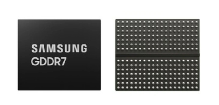
The official website of Samsung Electronics announced that it has completed the development of the industry's first graphics Double data rate 7 (GDDR7) DRAM. This year, it will first be installed on the next generation systems of major customers for verification. It is reported that this product is expected to be extended to future applications such as artificial intelligence, High-performance computing (HPC) and automobiles.


According to the official website, Samsung Electronics GDDR7 can achieve a bandwidth of 1.5 Terabyte per second (TBps), 1.4 times that of GDDR6 1.1TBps, and the speed of each data I/O (input/output) port can reach 32Gbps. This product adopts pulse amplitude modulation (PAM3) signal method, replacing the non return to zero (NRZ) signal method of previous generations of products, to improve performance. Within the same signal cycle, the PAM3 signal method can transmit 50% more data than the NRZ signal method.

未标题-1

Samsung GDDR7 graphics memory


Compared to GDDR6, the design of GDDR7 adopts energy-saving technology suitable for high-speed operation, which improves energy efficiency by 20%. Samsung Electronics offers a low operating voltage option for devices that focus on power consumption, such as laptops.


After Samsung Electronics developed the GDDR6 16Gb with a speed of 24 gigabits per second (Gbps) in 2022, the GDDR7 16Gb product will provide Samsung Electronics' highest graphics memory speed of 32Gbps to date. The innovation in integrated circuit (IC) design and packaging technology has improved performance stability under high-speed operation.


Yongcheol Bae, executive vice president of Samsung's electronic memory product planning team, said that the company's GDDR7 products will help improve the user experience that needs high-performance video storage, such as workstations, personal computers and game consoles, and are expected to expand to future applications such as artificial intelligence, High-performance computing and automobiles. The new generation of graphics memory will be pushed to the market according to demand, and the company hopes to continue to maintain cutting-edge technological capabilities in this field.

Hot news
Differences in the Performance of LED Core Technologies
The core performance indicators of LED devices are mainly reflected in the following six aspects
PCB wiring principles and techniques
1、 Manually wiring as much as possible
Mikroe Motion 2 Click Board Product Introduction
Mikroe Motion 2 Click is based on the Panasonic EKMC1607112 PIR motion sensor and is used as a human motion detector
SK Hynix develops a new generation of mobile NAND flash memory solutions
As the industry's highest-performance product, it will begin mass production in the third quarter of this year and be integrated into edge-side AI smartphones
Samsung is about to mass produce Galaxy Tab S10
According to media reports, Samsung is about to launch a new generation of Galaxy Tab S10 series, which is testing the Galaxy Tab S10+equipped with MediaTek Dimensity 9300+, changing the previous strategy of Qualcomm Snapdragon chip monopoly.
Samsung announces chip manufacturing technology roadmap
According to reports, Samsung Electronics announced its technology roadmap for chip manufacturing at its annual foundry forum held at its US chip headquarters in San Jose, California, with the aim of enhancing its competitiveness in the artificial intelligence chip foundry market through a series of upcoming technological advancements. Despite Samsung's strong position as a leading global memory chip manufacturer, it has always faced strong challenges from competitors such as TSMC in the field of wafer foundry.
NXP and World Advanced Plan Invest $7.8 billion in Singapore to Build a Wafer Factory
On June 5th, World Advanced and NXP Semiconductors announced plans to jointly establish the VisionPower Semiconductor Manufacturing Company (VSMC) joint venture in Singapore to build a 12 inch (300mm) wafer fab. The wafer factory has an investment of approximately 7.8 billion US dollars, with World Advanced investing 2.4 billion US dollars to hold 60% equity, and NXP investing 1.6 billion US dollars to hold 40% equity.
Mitsubishi Electric Kumamoto Prefecture SiC Wafer Factory to Start Production Ahead of Time
Recently, Mitsubishi Electric announced at a performance briefing that its SiC wafer plant located in Kumamoto Prefecture will be put into operation ahead of schedule due to strong market demand. The factory, originally scheduled to start operation in April 2026, will be put into production in November 2025, about 5 months ahead of schedule.
Passive component leader National Giant plans to transform into IDM company
In the past 5 to 10 years, Guoju has been steadily developing, consciously investing in new corporate groups through mergers and private equity investments.
Intel, Microsoft, Broadcom and other eight giants jointly launch the UALink standard
According to reports, Intel, Google, Microsoft, Meta, and other tech giants have announced the establishment of a new industry organization called "Ultra Accelerator Link (UALink) Promotion Group".
User Info:
Phone number
+86
  • +86
  • +886
  • +852
Company Name
Email
Product model
Quantity
Comment message